Description
Pin Name A0-A14 D0-D7 CE OE WE VCC VSS NC Pin Function Address Inputs Data Inputs/Outputs Chip Enable (Active Low) Output Enable (Active Low) Write Enable (Active Low) Power Ground Not Connected (Floating)
EM033C08 STSOP, TSOP
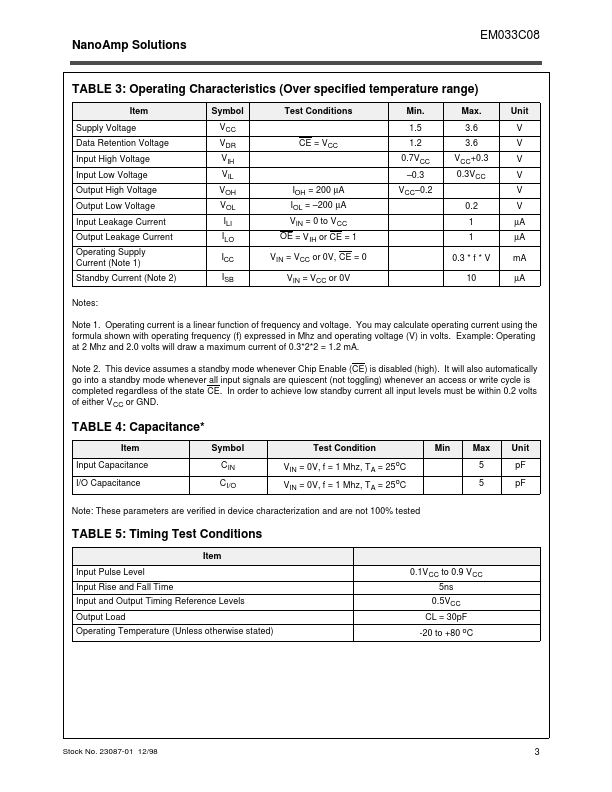
FIGURE 2: Operating Envelope
8 Mhz
8 Typical ICC (mA) 6
5 Mhz
4 2 0 0 1 2 VCC (V) 3 4
2.5 Mhz 1 Mhz
Stock No.23087-01 12/98
1
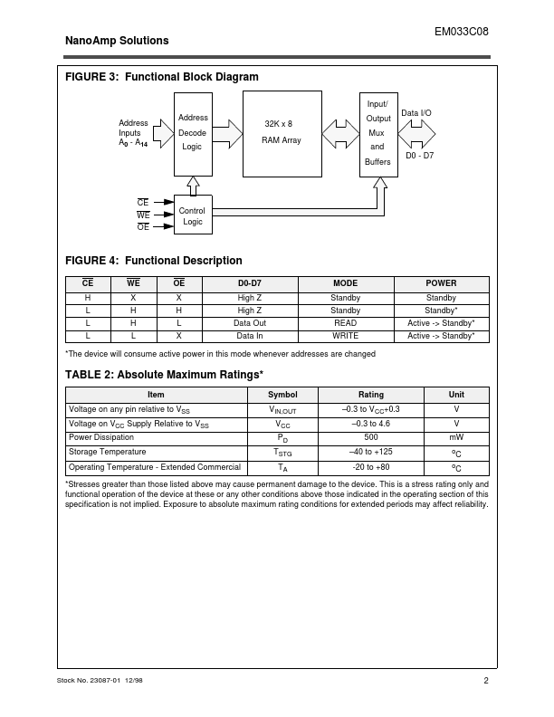
NanoAmp Solutions FIGURE 3: Functional Block Diagram
Input/ Address Inputs A0 - A14 Address Decode Logic 32K x 8 RAM Array Output Mux and
Features
- Extended Operating Voltage Range 1.5 to 3.6 V Very Low Standby Voltage 1.2 V Extended Temperature Range -20o to +80oC Fast Cycle Time 100 ns (@ 2.7V) Very Low Operating Current ICC < 1 mA typical at 3V, 1 Mhz Very Low Standby Current ISB = 100 nA typical Available in 32-pin STSOP or TSOP package
FIGURE 1: Pin Configuration
A11 A9 A8 A13 A14 NC CE VCC WE NC NC A12 A7 A6 A5 A4 1 2 3 4 5 6 7 8 9 10 11 12 13 14 15 16 32 31 30 29.
 EM033C08_IntegratedSiliconSolutionInc.pdf