Datasheet Details
| Part number | ICS9DB104 |
|---|---|
| Manufacturer | Integrated Circuit Systems |
| File Size | 263.73 KB |
| Description | Four Output Differential Buffer |
| Datasheet |
 ICS9DB104_IntegratedCircuitSystems.pdf ICS9DB104_IntegratedCircuitSystems.pdf
|
| Part number | ICS9DB104 |
|---|---|
| Manufacturer | Integrated Circuit Systems |
| File Size | 263.73 KB |
| Description | Four Output Differential Buffer |
| Datasheet |
ICS9DB104_IntegratedCircuitSystems.pdf
|
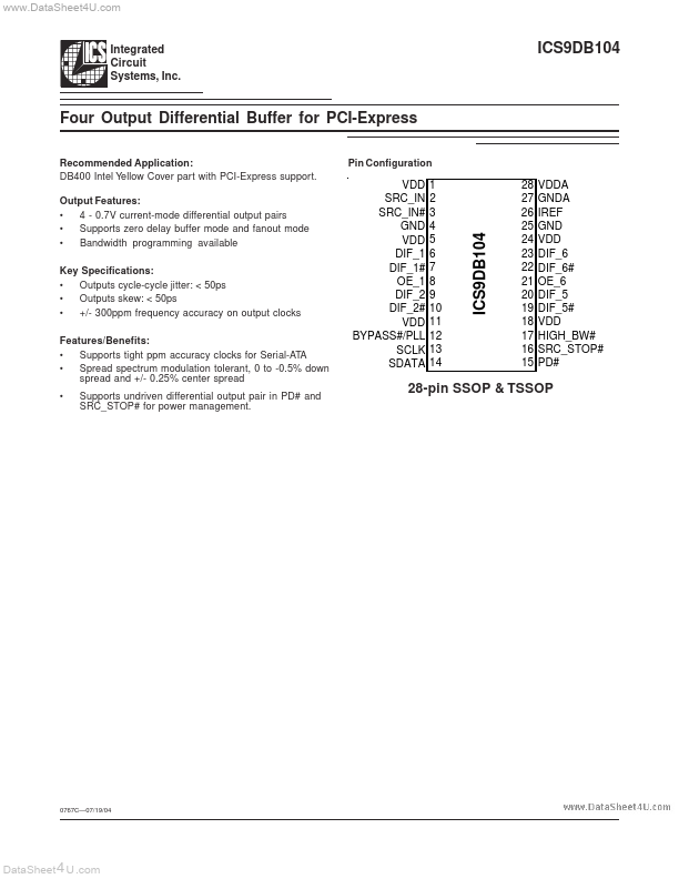
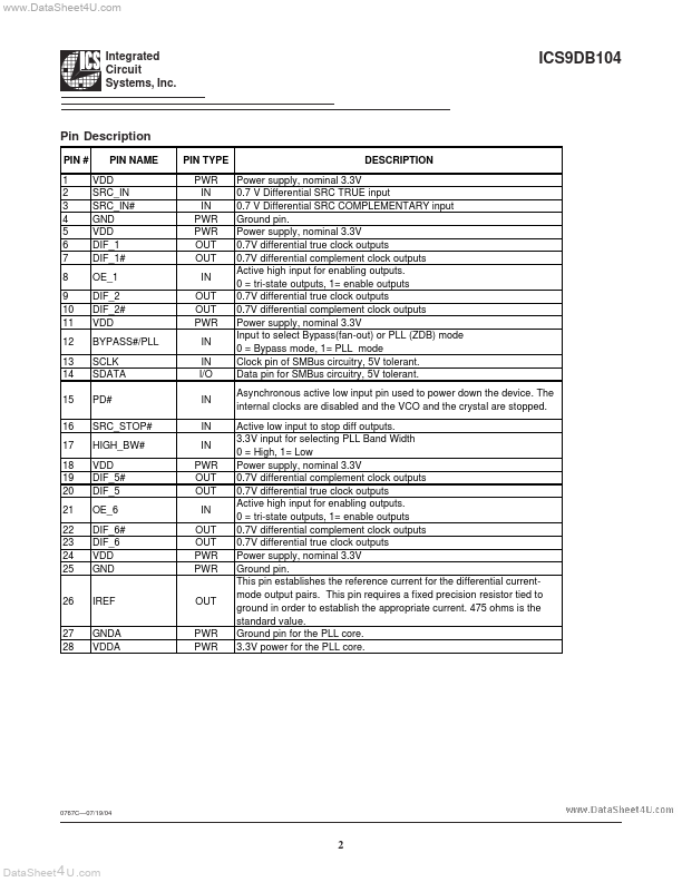
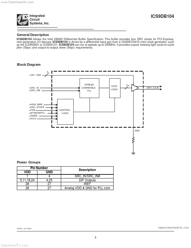
PIN # 1 2 3 4 5 6 7 8 9 10 11 12 13 14 15 16 17 18 19 20 21 22 23 24 25 26 27 28 PIN NAME VDD SRC_IN SRC_IN# GND VDD DIF_1 DIF_1# OE_1 DIF_2 DIF_2# VDD BYPASS#/PLL SCLK SDATA PD# SRC_STOP# HIGH_BW# VDD DIF_5# DIF_5 OE_6 DIF_6# DIF_6 VDD GND IREF GNDA VDDA PIN TYPE PWR IN IN PWR PWR OUT OUT IN OUT OUT PWR IN IN I/O IN IN IN PWR OUT OUT IN OUT OUT PWR PWR OUT PWR PWR DESCRIPTION Power supply, nominal 3.3V 0.7 V Differential SRC TRUE input 0.7 V Differential SRC COMPLEMENTARY input Ground pin.
📁 ICS9DB104 Similar Datasheet