Datasheet Details
| Part number | ICS9DBL411 |
|---|---|
| Manufacturer | IDT |
| File Size | 111.89 KB |
| Description | Four Output Differential Fanout Buffer |
| Datasheet |
 ICS9DBL411_IDT.pdf ICS9DBL411_IDT.pdf
|
| Part number | ICS9DBL411 |
|---|---|
| Manufacturer | IDT |
| File Size | 111.89 KB |
| Description | Four Output Differential Fanout Buffer |
| Datasheet |
ICS9DBL411_IDT.pdf
|
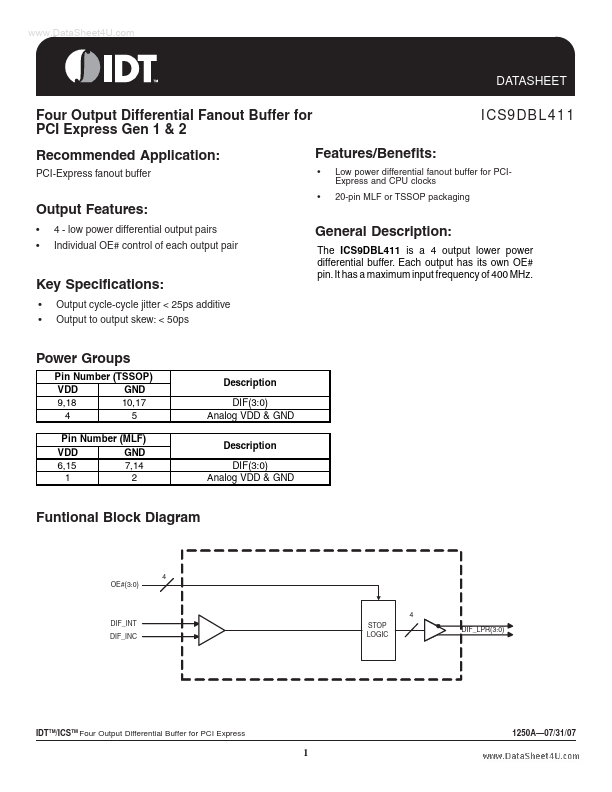
The ICS9DBL411 is a 4 output lower power differential buffer. Output cycle-cycle jitter < 25ps additive Output to output skew: < 50ps Power Groups Pin Number (TSSOP) VDD GND 9,18 10,17 4 5 Pin Number (MLF) VDD GND 6,15 7,14 1 2 Description DIF(3:0) Analog VDD & GND Description DIF(3:0) Analog VDD & GND Funtional Block Diagram 4 OE#(3:0) 4 DIF_INT DIF_INC STOP LOGIC DIF_LPR(
📁 ICS9DBL411 Similar Datasheet