Description
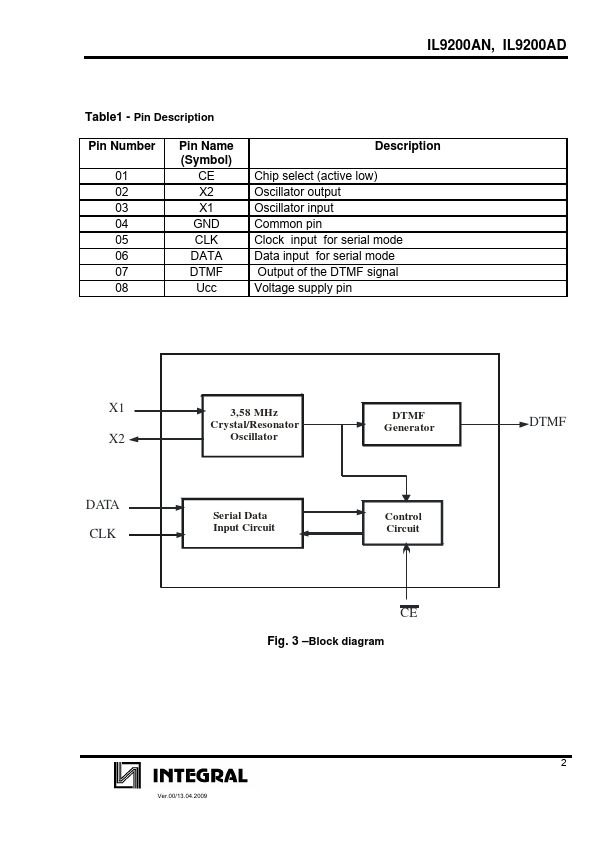
Pin Number
01 02 03 04 05 06 07 08
Pin Name (Symbol)
CE Х2 Х1 GND CLK DATA DTMF Ucc
Description
Chip select (active low) Oscillator output Oscillator input Common pin Clock input for serial mode Data input for serial mode Output of the DTMF signal Voltage supply pin
X1 X2
DATA CLK
3,58 MHz Crystal/Resonator
Oscillator
Serial Data Input Circuit
DTMF Generator
Control Circuit
CE
Fig.3
Block diagram
DTMF
Ver.00/13.04.2009
2
Table 2
Absolute maximum ratings
Symbol
UCC
Features
- Supply voltage Ucc from 2,0 to 5,5 V;.
- Serial mode of data input;.
- Clock frequency 3,58 MHz;.
- Low standby current consumption;.
- Internal timer for writing;.
- Low total harmonic distortion ;.
- Operating temperature from -20 to 75 oC
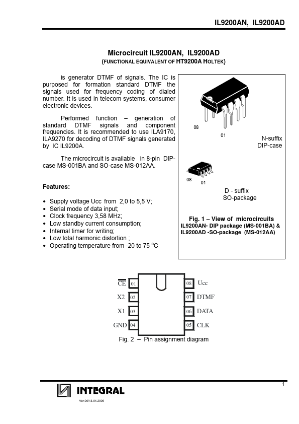
08 01
D - suffix SO-package
Fig. 1.
- View of microcircuits
IL9200AN- DIP package (MS-001BA) & IL9200AD -SO-package (MS-012AA)
CE 01
08 Ucc
X2 02
07 DTMF
X1 03
06 DATA
GND 04
05 CLK
Fig.
 IL9200AN-Integral.pdf