Datasheet4U Logo Datasheet4U.com

IS61QDP2B22M18A2 - 36Mb QUADP (Burst 2) Synchronous SRAM

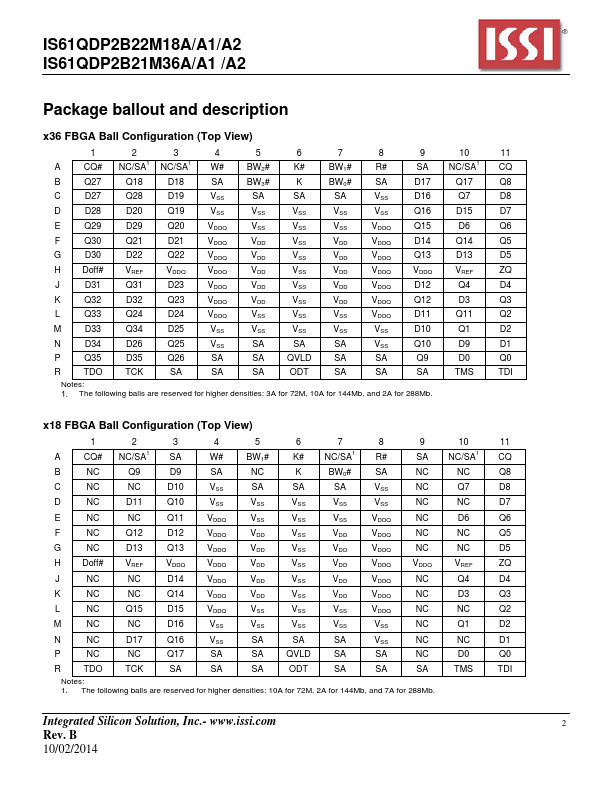
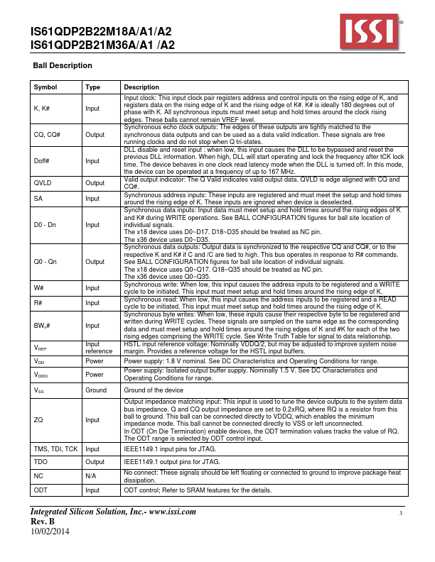
This page provides the datasheet information for the IS61QDP2B22M18A2, a member of the IS61QDP2B22M18A 36Mb QUADP (Burst 2) Synchronous SRAM family.

Description

devices.

need for high-speed bus turnaround.

operations are self-timed.

Features

  • 1Mx36 and 2Mx18 configuration available.
  • On-chip Delay-Locked Loop (DLL) for wide data valid window.
  • Separate independent read and write ports with concurrent read and write operations.
  • Synchronous pipeline read with EARLY write operation.
  • Double Data Rate (DDR) interface for read and write input ports.
  • 2.0 Cycle read latency.
  • Fixed 2-bit burst for read and write operations.
  • Clock stop support.
  • Two input clocks (K and K#) for address and cont.

📥 Download Datasheet

Datasheet preview – IS61QDP2B22M18A2

Datasheet Details

Part number IS61QDP2B22M18A2
Manufacturer ISSI (now Infineon)
File Size 660.37 KB
Description 36Mb QUADP (Burst 2) Synchronous SRAM
Datasheet download datasheet IS61QDP2B22M18A2 Datasheet
Additional preview pages of the IS61QDP2B22M18A2 datasheet.
Other Datasheets by ISSI

Full PDF Text Transcription

Click to expand full text
IS61QDP2B22M18A/A1/A2 IS61QDP2B21M36A/A1/A2 2Mx18, 1Mx36 36Mb QUADP (Burst 2) Synchronous SRAM (2.0 CYCLE READ LATENCY) JANUARY 2015 FEATURES  1Mx36 and 2Mx18 configuration available.  On-chip Delay-Locked Loop (DLL) for wide data valid window.  Separate independent read and write ports with concurrent read and write operations.  Synchronous pipeline read with EARLY write operation.  Double Data Rate (DDR) interface for read and write input ports.  2.0 Cycle read latency.  Fixed 2-bit burst for read and write operations.  Clock stop support.  Two input clocks (K and K#) for address and control registering at rising edges only.  Two echo clocks (CQ and CQ#) that are delivered simultaneously with data.
Published: |