Datasheet Details
| Part number | 8SLVD1204-33 |
|---|---|
| Manufacturer | IDT |
| File Size | 513.19 KB |
| Description | LVDS Output Fanout Buffer |
| Datasheet |
 8SLVD1204-33 Datasheet 8SLVD1204-33 Datasheet
|
|
|
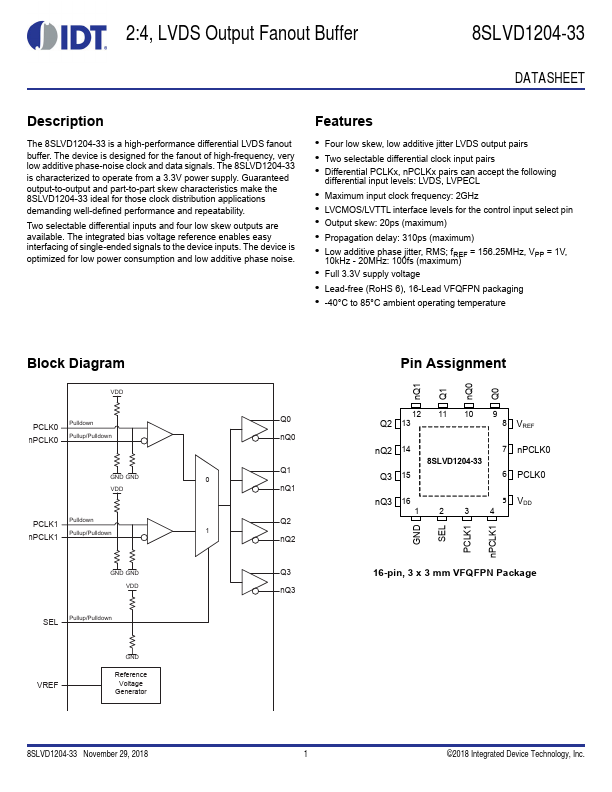
The 8SLVD1204-33 is a high-performance differential LVDS fanout buffer.
The device is designed for the fanout of high-frequency, very low additive phase-noise clock and data signals.
The 8SLVD1204-33 is characterized to operate from a 3.3V power supply.
| Part number | 8SLVD1204-33 |
|---|---|
| Manufacturer | IDT |
| File Size | 513.19 KB |
| Description | LVDS Output Fanout Buffer |
| Datasheet |
8SLVD1204-33 Datasheet
|
|
|
|
| Part Number | Description | Manufacturer |
|---|---|---|
| 8SLVD1204 | LVDS Output Fanout Buffer | Renesas |
| 8SLVD1212 | LVDS fanout buffer | Renesas |
| 8SLVD2102 | Dual 1:2 LVDS Output Fanout Buffer | Renesas |
| 8SLVP1102 | 2.5V LVPECL Output Fanout Buffer | Renesas |
| 8SLVP1204 | LVPECL Output Fanout Buffer | Renesas |
| Part Number | Description |
|---|---|
| 8SLVD1212 | LVDS Output Fanout Buffer |
| 8SLVD2102 | LVDS Output Fanout Buffer |
| 8SLVD2104 | LVDS Output Fanout Buffer |
| 8SLVP1204 | LVPECL Output Fanout Buffer |
| 8SLVP1208 | LVPECL Output Fanout Buffer |
The following content is an automatically extracted verbatim text from the original manufacturer datasheet and is provided for reference purposes only.