Download the GS8342D08E-300 datasheet PDF.
This datasheet also covers the GS8342D08E-333 variant, as both devices belong to the same 36mb sigmaquad-ii burst family and are provided as variant models within a single manufacturer datasheet.
Description
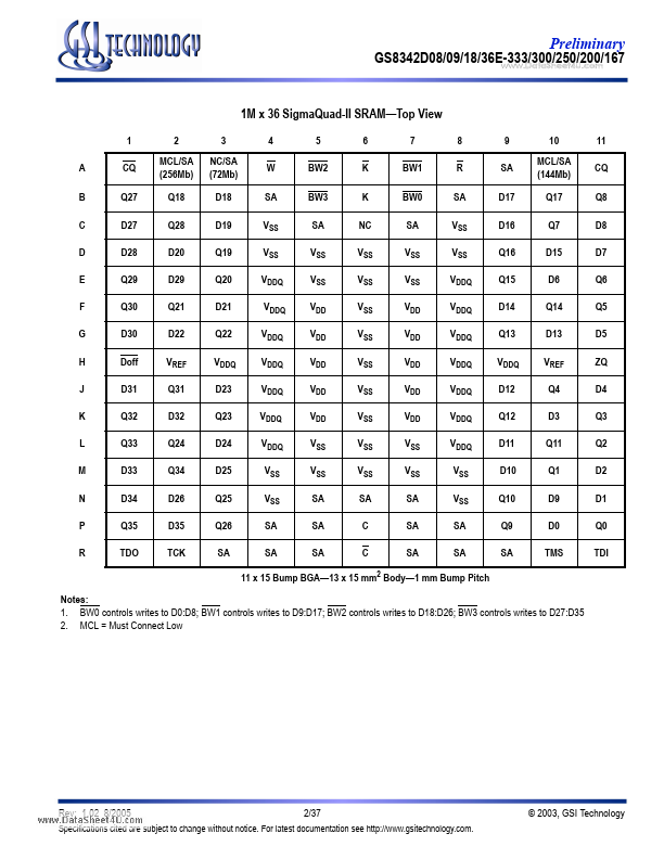
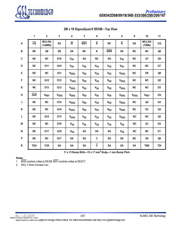
Table Symbol
SA NC R W BW0
BW3 NW0
NW1 K K C C TMS TDI TCK TDO VREF ZQ Qn Dn Doff CQ CQ VDD VDDQ VSS Note: NC = Not Connected to die or any other pin
Description
Synchronous Address Inputs No Connect Synchronous Read Synchronous Write Synchronous Byte Writes Nybble Write Control Pin
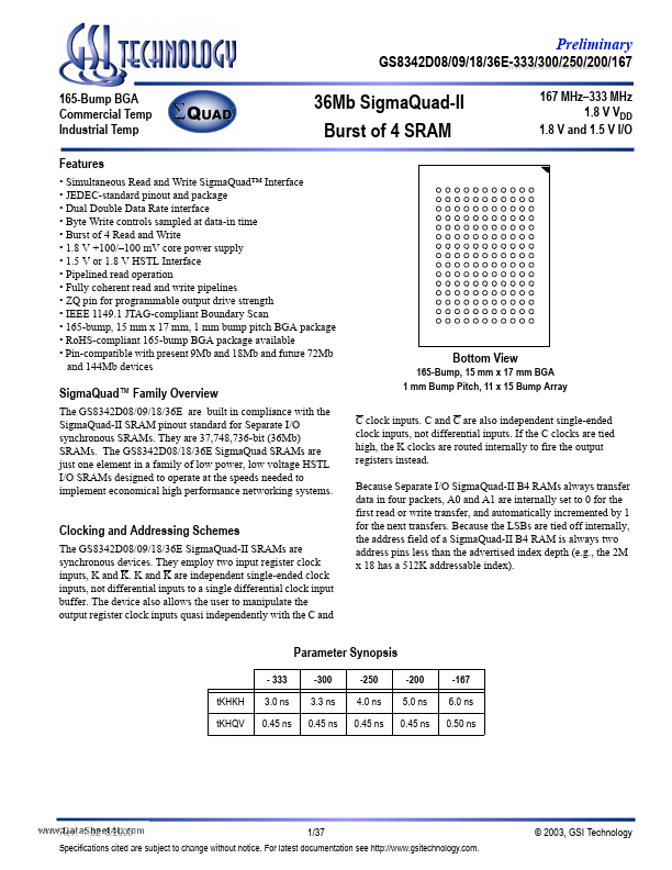
Features
- Simultaneous Read and Write SigmaQuad™ Interface.
- JEDEC-standard pinout and package.
- Dual Double Data Rate interface.
- Byte Write controls sampled at data-in time.
- Burst of 4 Read and Write.
- 1.8 V +100/.
- 100 mV core power supply.
- 1.5 V or 1.8 V HSTL Interface.
- Pipelined read operation.
- Fully coherent read and write pipelines.
- ZQ pin for programmable output drive strength.
- IEEE 1149.1 JTAG-co.
 GS8342D08E-300 Datasheet