GS8342D08E-250 Datasheet Summary
Preliminary GS8342D08/09/18/36E-333/300/250/200/167 ..
165-Bump BGA mercial Temp Industrial Temp Features
- Simultaneous Read and Write SigmaQuad™ Interface
- JEDEC-standard pinout and package
- Dual Double Data Rate interface
- Byte Write controls sampled at data-in time
- Burst of 4 Read and Write
- 1.8 V +100/- 100 mV core power supply
- 1.5 V or 1.8 V HSTL Interface
- Pipelined read operation
- Fully coherent read and write pipelines
- ZQ pin for programmable output drive strength
- IEEE 1149.1 JTAG-pliant Boundary Scan
- 165-bump, 15 mm x 17 mm, 1 mm bump pitch BGA package
- RoHS-pliant 165-bump BGA package available
- Pin-patible with present 9Mb and 18Mb and future 72Mb and 144Mb devices
36Mb SigmaQuad-II Burst of 4 SRAM
167 MHz- 333 MHz 1.8 V VDD 1.8 V and 1.5 V I/O
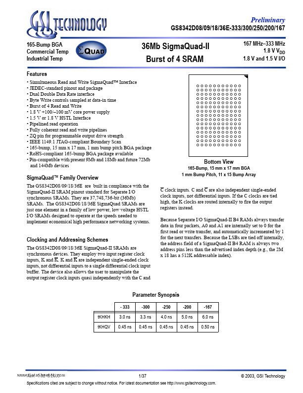
Bottom View
165-Bump, 15 mm x 17 mm BGA 1 mm Bump Pitch, 11 x 15 Bump Array C clock inputs. C and C are also independent single-ended clock inputs, not differential inputs. If the C clocks are tied high, the K clocks are routed internally to fire the output registers instead. Because Separate I/O SigmaQuad-II B4 RAMs always transfer data in four packets, A0 and A1 are internally set to 0 for the first read or write transfer, and automatically incremented by 1 for the next transfers. Because the LSBs are tied off internally, the address field of a SigmaQuad-II B4 RAM is always two address pins less than the advertised index depth (e.g., the 2M x 18 has a 512K addressable index).
SigmaQuad™ Family Overview
The GS8342D08/09/18/36E are built in pliance with the SigmaQuad-II SRAM pinout standard for Separate I/O synchronous SRAMs. They are 37,748,736-bit (36Mb) SRAMs. The GS8342D08/18/36E SigmaQuad SRAMs are just one element in a family of low power, low voltage HSTL...