Datasheet4U Logo Datasheet4U.com

MRF7S16150HSR3 - RF Power Field Effect Transistors

Download the MRF7S16150HSR3 datasheet PDF. This datasheet also covers the MRF7S16150HR3 variant, as both devices belong to the same rf power field effect transistors family and are provided as variant models within a single manufacturer datasheet.

Description

Small Ferrite Bead 10 μF, 35 V Electrolytic Capacitor 0.01 μF, 50 V Chip Capacitors 10 pF Chip Capacitors 47 pF Chip Capacitors 22 μF, 35 V Tantalum Capacitors 220 μF, 50 V Electrolytic Capacitor 1 KΩ, 1/4 W Chip Resistor 10 Ω, 1/4 W Chip Resistor Part Number 2743019447 EMVY350ADA100ME55G C1825C103J

Features

  • Characterized with Series Equivalent Large - Signal Impedance Parameters.
  • Internally Matched for Ease of Use.
  • Integrated ESD Protection.
  • Greater Negative Gate - Source Voltage Range for Improved Class C Operation.
  • RoHS Compliant.
  • In Tape and Reel. R3 Suffix = 250 Units per 56 mm, 13 inch Reel. MRF7S16150HR3 MRF7S16150HSR3 1600- 1660 MHz, 32 W AVG. , 28 V WiMAX.

📥 Download Datasheet

Note: The manufacturer provides a single datasheet file (MRF7S16150HR3_FreescaleSemiconductor.pdf) that lists specifications for multiple related part numbers.

Full PDF Text Transcription (Reference)

The following content is an automatically extracted verbatim text from the original manufacturer datasheet and is provided for reference purposes only.

View original datasheet text
www.DataSheet4U.com 
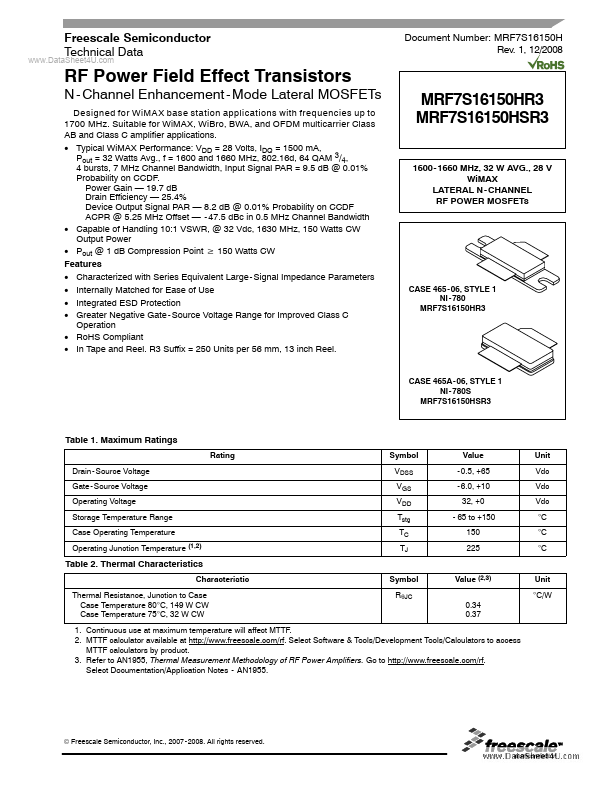
Freescale Semiconductor Technical Data Document Number: MRF7S16150H Rev. 1, 12/2008 RF Power Field Effect Transistors N - Channel Enhancement - Mode Lateral MOSFETs Designed for WiMAX base station applications with frequencies up to 1700 MHz. Suitable for WiMAX, WiBro, BWA, and OFDM multicarrier Class AB and Class C amplifier applications. • Typical WiMAX Performance: VDD = 28 Volts, IDQ = 1500 mA, Pout = 32 Watts Avg., f = 1600 and 1660 MHz, 802.16d, 64 QAM 3/4, 4 bursts, 7 MHz Channel Bandwidth, Input Signal PAR = 9.5 dB @ 0.01% Probability on CCDF. Power Gain — 19.7 dB Drain Efficiency — 25.4% Device Output Signal PAR — 8.2 dB @ 0.01% Probability on CCDF ACPR @ 5.25 MHz Offset — - 47.5 dBc in 0.
Published: |