Click to expand full text
Freescale Semiconductor Technical Data
Document Number: MD7IC21100N Rev. 0, 10/2008
www.DataSheet4U.com
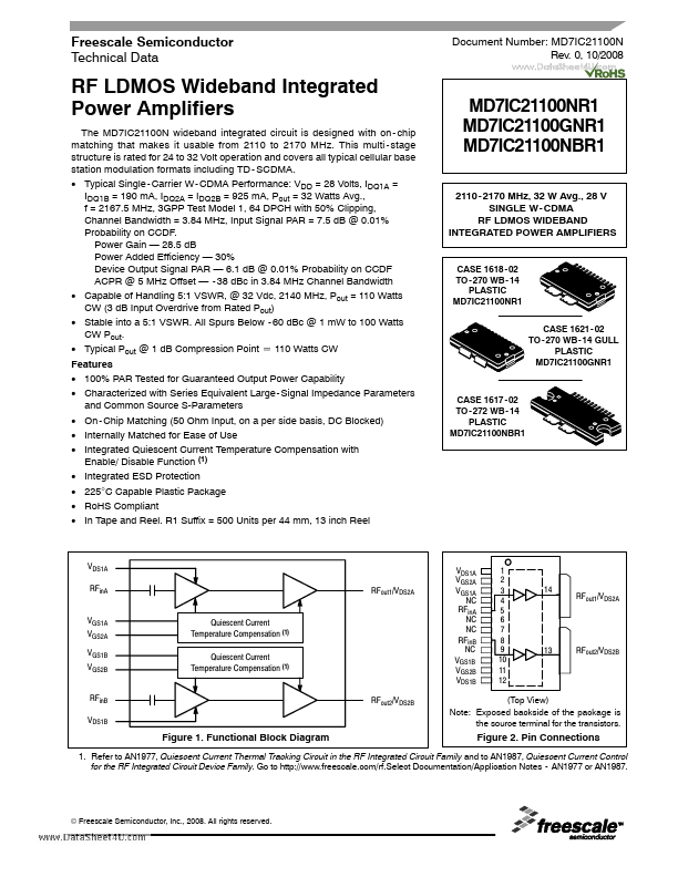
RF LDMOS Wideband Integrated Power Amplifiers
The MD7IC21100N wideband integrated circuit is designed with on - chip matching that makes it usable from 2110 to 2170 MHz. This multi - stage structure is rated for 24 to 32 Volt operation and covers all typical cellular base station modulation formats including TD - SCDMA. • Typical Single- Carrier W - CDMA Performance: VDD = 28 Volts, IDQ1A = IDQ1B = 190 mA, IDQ2A = IDQ2B = 925 mA, Pout = 32 Watts Avg., f = 2167.5 MHz, 3GPP Test Model 1, 64 DPCH with 50% Clipping, Channel Bandwidth = 3.84 MHz, Input Signal PAR = 7.5 dB @ 0.01% Probability on CCDF. Power Gain — 28.5 dB Power Added Efficiency — 30% Device Output Signal PAR — 6.1 dB @ 0.
 MD7IC21100GNR1 Datasheet