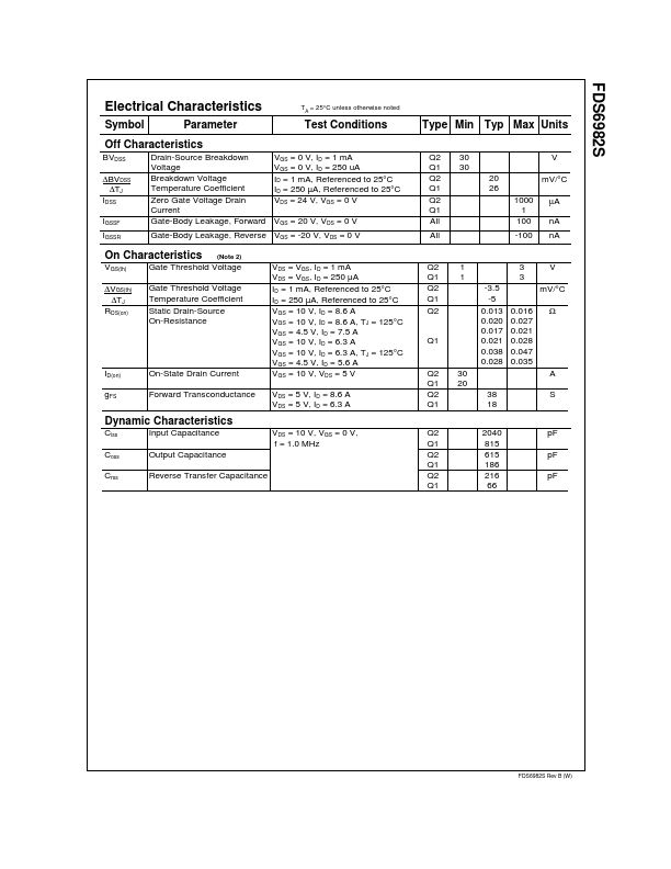
Datasheet4U Logo Datasheet4U.com

FDS6982S - Dual N-Channel MOSFET

Description

The FDS6982S is designed to replace two single SO-8 MOSFETs and Schottky diode in synchronous DC:DC power supplies that provide various peripheral voltages for notebook computers and other battery powered electronic devices.

Features

  • Q2: Optimized to minimize conduction losses Includes SyncFET Schottky body diode RDS(on) = 0.016Ω @ VGS = 10V RDS(on) = 0.021Ω @ VGS = 4.5V.
  • Q1: Optimized for low switching losses Low Gate Charge ( 8.5 nC typical) RDS(on) = 0.028Ω @ VGS = 10V RDS(on) = 0.035Ω @ VGS = 4.5V 8.6A, 30V 6.3A, 30V D1 D1 D2 D2 S1 G1 5 6 7 Q1 4 3 2 Q2 SO-8 S2 8 1 G2 Absolute Maximum Ratings Symbol VDSS VGSS ID PD Drain-Source Voltage Gate-Source Voltage Drain Current TA = 25°C unless otherwi.

📥 Download Datasheet

Full PDF Text Transcription (Reference)

The following content is an automatically extracted verbatim text from the original manufacturer datasheet and is provided for reference purposes only.

View original datasheet text
FDS6982S March 2000 PRELIMINARY FDS6982S Dual Notebook Power Supply N-Channel PowerTrench SyncFet™ General Description The FDS6982S is designed to replace two single SO-8 MOSFETs and Schottky diode in synchronous DC:DC power supplies that provide various peripheral voltages for notebook computers and other battery powered electronic devices. FDS6982S contains two unique 30V, N-channel, logic level, PowerTrench MOSFETs designed to maximize power conversion efficiency. The high-side switch (Q1) is designed with specific emphasis on reducing switching losses while the lowside switch (Q2) is optimized to reduce conduction losses. Q2 also includes an integrated Schottky diode using Fairchild’s monolithic SyncFET technology.
Published: |