Datasheet Details
| Part number | FDC6320C |
|---|---|
| Manufacturer | Fairchild Semiconductor (now onsemi) |
| File Size | 100.14 KB |
| Description | Dual N & P Channel / Digital FET |
| Datasheet |
 FDC6320C Datasheet FDC6320C Datasheet
|
|
|
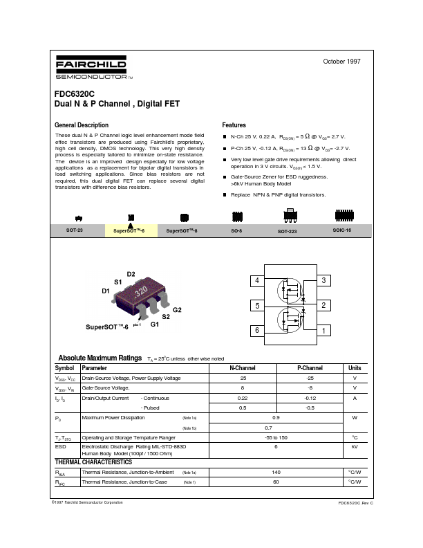
These dual N & P Channel logic level enhancement mode field effec transistors are produced using Fairchild's proprietary, high cell density, DMOS technology.
This very high density process is especially tailored to minimize on-state resistance.
| Part number | FDC6320C |
|---|---|
| Manufacturer | Fairchild Semiconductor (now onsemi) |
| File Size | 100.14 KB |
| Description | Dual N & P Channel / Digital FET |
| Datasheet |
FDC6320C Datasheet
|
|
|
|