The following content is an automatically extracted verbatim text
from the original manufacturer datasheet and is provided for reference purposes only.
View original datasheet text
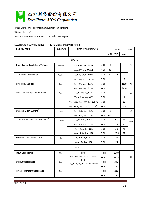
N & P‐Channel Logic Level Enhancement Mode Field Effect Transistor
Product Summary:
N‐CH
P‐CH
BVDSS
30V
‐30V
RDSON (MAX.)
6.5mΩ 20mΩ
ID
26A
‐15A
UIS, Rg 100% Tested Pb‐Free Lead Plating & Halogen Free
ABSOLUTE MAXIMUM RATINGS (TC = 25 °C Unless Otherwise Noted)
PARAMETERS/TEST CONDITIONS
SYMBOL
Gate‐Source Voltage
VGS
Continuous Drain Current Pulsed Drain Current1
TC = 25 °C TC = 100 °C
Avalanche Current
Avalanche Energy
L = 0.1mH, ID=15A, RG=25Ω(N) L = 0.1mH, ID=‐10A, RG=25Ω(P)
Repetitive Avalanche Energy2
L = 0.
 EMB20D03H Datasheet