Datasheet4U Logo Datasheet4U.com

EM562161 - 128K x 16 Low Power SRAM

Description

Symbol A0 - A16 DQ0 - DQ15 CE1#, CE2 OE# WE# LB#, UB# GND VDD NC Function Address Inputs Data Inputs / Outputs Chip Enable Inputs Output Enable Read / Write Control Input Data Byte Control Inputs Ground Power Supply No Connection A LB # O E# A0 A1 A2 CE 2 B DQ 8 UB # A3 A4 CE1 # DQ 0

Features

  • Single power supply voltage of 2.7V to 3.6V.
  • Power down features using CE1# and CE2.
  • Low operating current : 30mA(max for 55 ns).
  • Maximum Standby current : 10µA at 3.6 V.
  • Data retention supply voltage: 1.5V to 3.6V.
  • Direct TTL compatibility for all input and output.
  • Wide operating temperature range: -40°C to 85°C.
  • Package type: 48-ball TFBGA, 6x8mm EM562161 128K x 16 Low Power SRAM Preliminary, Rev 1.0 07/2001 circuit tec.

📥 Download Datasheet

Datasheet Details

Part number EM562161
Manufacturer Etron Technology
File Size 140.13 KB
Description 128K x 16 Low Power SRAM
Datasheet download datasheet EM562161 Datasheet
Other Datasheets by Etron Technology

Full PDF Text Transcription

Click to expand full text
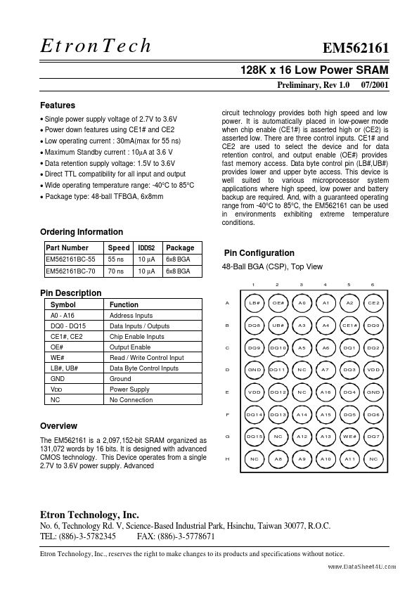
EtronTech Features • Single power supply voltage of 2.7V to 3.6V • Power down features using CE1# and CE2 • Low operating current : 30mA(max for 55 ns) • Maximum Standby current : 10µA at 3.6 V • Data retention supply voltage: 1.5V to 3.6V • Direct TTL compatibility for all input and output • Wide operating temperature range: -40°C to 85°C • Package type: 48-ball TFBGA, 6x8mm EM562161 128K x 16 Low Power SRAM Preliminary, Rev 1.0 07/2001 
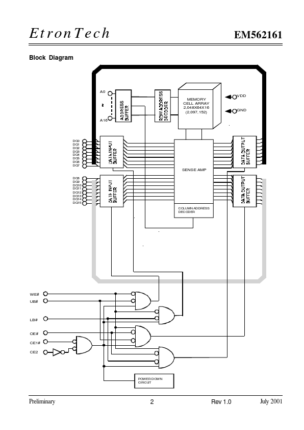
circuit technology provides both high speed and low power. It is automatically placed in low-power mode when chip enable (CE1#) is asserted high or (CE2) is asserted low. There are three control inputs. CE1# and CE2 are used to select the device and for data retention control, and output enable (OE#) provides fast memory access.
Published: |