Datasheet Details
| Part number | FM25V40 |
|---|---|
| Manufacturer | Cypress Semiconductor |
| File Size | 557.51 KB |
| Description | 4-Mbit (512K x 8) Serial (SPI) F-RAM |
| Datasheet |
 FM25V40-CypressSemiconductor.pdf FM25V40-CypressSemiconductor.pdf
|
| Part number | FM25V40 |
|---|---|
| Manufacturer | Cypress Semiconductor |
| File Size | 557.51 KB |
| Description | 4-Mbit (512K x 8) Serial (SPI) F-RAM |
| Datasheet |
FM25V40-CypressSemiconductor.pdf
|
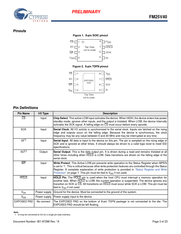
CS Input Chip Select.This active LOW input activates the device.When HIGH, the device enters low-power standby mode, ignores other inputs, and the output is tristated.When LOW, the device internally activates the SCK signal.A falling edge on CS must occur before every opcode.SCK SI[1] SO[1] Input Input Output Serial Clock.All I/O activity is synchronized to the serial clock.Inputs are latched on the rising edge and outputs occur on the falling edge.Because the device is synchrono
📁 FM25V40 Similar Datasheet