Datasheet Details
| Part number | CY7C1360V25 |
|---|---|
| Manufacturer | Cypress (Infineon) |
| File Size | 411.27 KB |
| Description | 256K x 36/256K x 32/512K x 18 Pipelined SRAM |
| Datasheet |
 CY7C1360V25 Datasheet CY7C1360V25 Datasheet
|
|
|
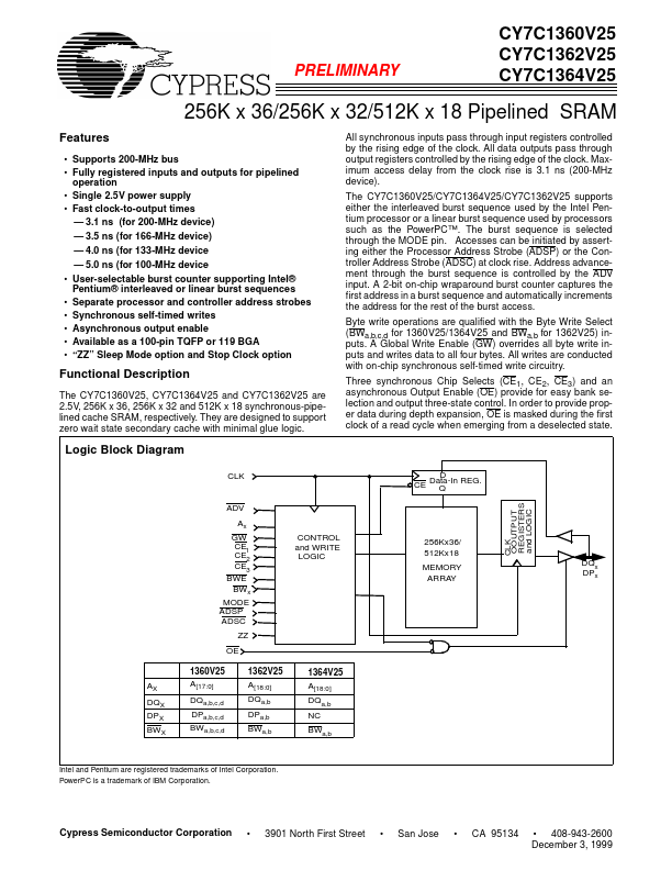
The CY7C1360V25, CY7C1364V25 and CY7C1362V25 are 2.5V, 256K x 36, 256K x 32 and 512K x 18 synchronous-pipelined cache SRAM, respectively.
They are designed to support zero wait state secondary cache with minimal glue logic.
| Part number | CY7C1360V25 |
|---|---|
| Manufacturer | Cypress (Infineon) |
| File Size | 411.27 KB |
| Description | 256K x 36/256K x 32/512K x 18 Pipelined SRAM |
| Datasheet |
CY7C1360V25 Datasheet
|
|
|
|
| Part Number | Description | Manufacturer |
|---|---|---|
| CY7C136AE | 1K/2K x 8 Dual-Port Static RAM | Cypress |
| CY7C136E | 1K/2K x 8 Dual-Port Static RAM | Cypress |
| CY7C131AE | 1K/2K x 8 Dual-Port Static RAM | Cypress |
| CY7C131E | 1K/2K x 8 Dual-Port Static RAM | Cypress |
| CY7C1370C | 512K x 36/1M x 18 Pipelined SRAM with NoBL Architecture | Cypress |
| Part Number | Description |
|---|---|
| CY7C1360C | 9-Mbit Pipelined SRAM |
| CY7C136 | 2K x 8 Dual-Port Static RAM |
| CY7C1361C | (CY7C1361C / CY7C1363C) 9-Mbit (256K x 36/512K x 18) Flow-Through SRAM |
| CY7C1362C | 9-Mbit Pipelined SRAM |
| CY7C1362V25 | 256K x 36/256K x 32/512K x 18 Pipelined SRAM |
The following content is an automatically extracted verbatim text from the original manufacturer datasheet and is provided for reference purposes only.