Datasheet Details
| Part number | 74LVC2G241 |
|---|---|
| Manufacturer | Nexperia |
| File Size | 269.27 KB |
| Description | Dual buffer/line driver |
| Datasheet |
 74LVC2G241 Datasheet 74LVC2G241 Datasheet
|
|
|
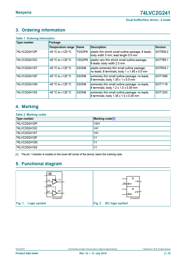
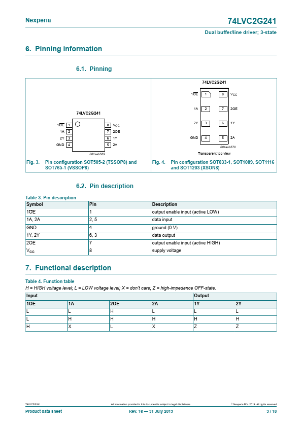
The 74LVC2G241 is a dual non-inverting buffer/line driver with 3-state outputs.
A HIGH level at pin 1OE causes output 1Y to assume a high-impedance OFF-state.
A LOW level at pin 2OE causes output 2Y to as| Part number | 74LVC2G241 |
|---|---|
| Manufacturer | Nexperia |
| File Size | 269.27 KB |
| Description | Dual buffer/line driver |
| Datasheet |
74LVC2G241 Datasheet
|
|
|
|
| Part Number | Description | Manufacturer |
|---|---|---|
| 74LVC2G241 | Dual buffer/line driver | NXP Semiconductors |
| 74LVC2G240 | Dual inverting buffer/line driver | NXP Semiconductors |
| 74LVC2G00 | DUAL 2-INPUT NAND GATE | Diodes |
| 74LVC2G00 | Dual 2-input NAND gate | NXP |
| 74LVC2G00-Q100 | Dual 2-input NAND gate | NXP |
| Part Number | Description |
|---|---|
| 74LVC2G241-Q100 | Dual buffer/line driver |
| 74LVC2G240 | Dual inverting buffer/line driver |
| 74LVC2G240-Q100 | Dual inverting buffer/line driver |
| 74LVC2G00 | Dual 2-input NAND gate |
| 74LVC2G00-Q100 | Dual 2-input NAND gate |
The following content is an automatically extracted verbatim text from the original manufacturer datasheet and is provided for reference purposes only.