TPS566250
TPS566250 is 6-A Synchronous Step-Down Converter manufactured by Texas Instruments.
Features
- 1 Integrated FETs Optimized for Lower Duty Cycle Applications
- 44 mΩ (High Side) and 23 mΩ (Low Side)
- Output Voltage Range: 0.6 V to 1.87 V with 5.5-m V Feedback Voltage Step
- VID Control with Multibyte Interface with Read-Back
- ±1% Output Voltage at 25°C for VID Control at 12 V VIN / 1.1 V VOUT
- D-CAP2™ Control Mode
- Advanced Eco-mode™ for High Efficiency at Light
Load and Low Output Voltage Ripple
- 650-k Hz Switching Frequency
- Fixed Soft Start: 1 ms
- Monotonic Pre-Biased Soft Start
- Hiccup Timer for Overload Protection
2 Applications
- Media Processors for Consumer Applications: Digital TVs, Set Top Boxes
- System On-Chip Power
- High Density Power Distribution Systems
3 Description
The TPS566250 is a synchronous buck converter that enables system designers to plete the suite of various end equipment’s power bus regulators with a cost effective, low ponent count and low standby current solution.
After the initial power-up, the output voltage can be changed by codes sent to the IC via an I2C patible VID Control bus.
The main control loops of the TPS566250 use the DCAP2™ mode control which provides a fast transient response with no external pensation ponents. The adaptive on-time control supports seamless transition between PWM mode at higher load conditions and Advanced Eco-mode™ operation at light loads. Advanced Eco-mode™ allows the TPS566250 to maintain high efficiency during lighter load conditions. The TPS566250 is able to adapt to both low equivalent series resistance (ESR) output capacitors such as POSCAP or SP-CAP, and ultralow ESR, ceramic capacitors.
The device offers on chip overcurrent, undervoltage lockout and thermal shutdown protection.
Device Information(1)
PART NUMBER
PACKAGE
BODY SIZE (NOM)
HSOP (8)
4.90 mm x 3.90 mm
(1) For all available packages, see the orderable addendum at the end of the data sheet.
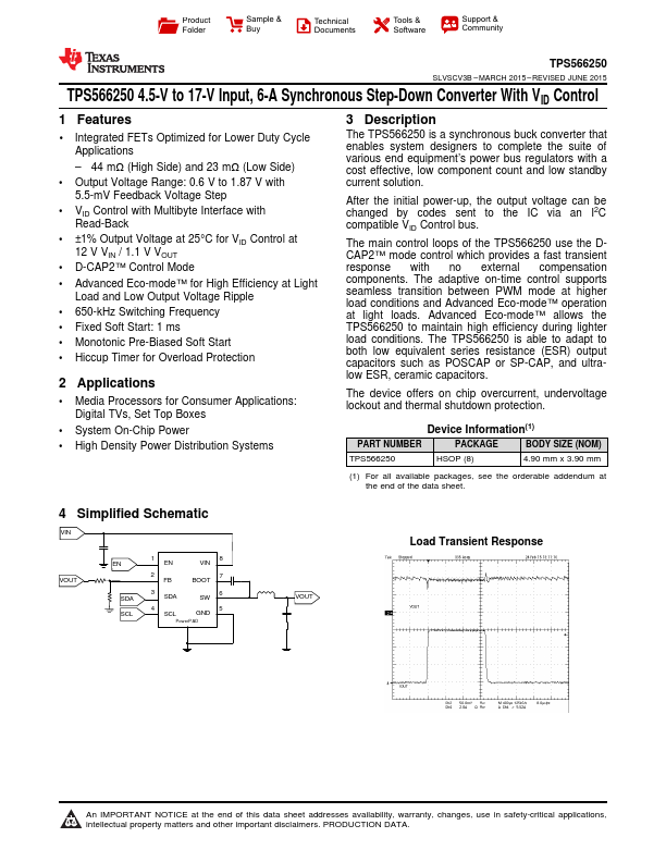
4 Simplified Schematic
VOUT
SDA SCL
1 EN
VIN 8
2 FB
7 BOOT
3 SDA
SW...