SN74LVC125A Overview
Key Specifications
Package: TSSOP
Mount Type: Surface Mount
Pins: 14
Max Voltage (typical range): 3.6 V
Description
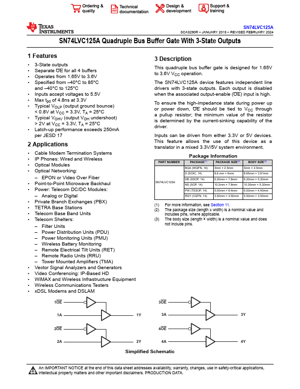
This quadruple bus buffer gate is designed for 1.65V to 3.6V VCC operation. The SN74LVC125A device features independent line drivers with 3-state outputs.
Key Features
- 3-State outputs
- Separate OE for all 4 buffers
- Operates from 1.65V to 3.6V
- Specified from –40°C to 85°C and –40°C to 125°C
- Inputs accept voltages to 5.5V