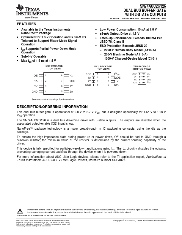
Download SN74AUC2G126 Datasheet PDF
SN74AUC2G126 page 2
Page 2
SN74AUC2G126 page 3
Page 3

SN74AUC2G126 Description

/ORDERING INFORMATION This dual bus buffer gate is operational at 0.8-V to 2.7-V VCC, but is designed specifically for 1.65-V to 1.95-V VCC operation. The SN74AUC2G126 is a dual bus driver/line driver with 3-state outputs. The outputs are disabled when the associated output-enable (OE) input is low.

SN74AUC2G126 Key Features

  • Available in the Texas Instruments NanoFree™ Package
  • Optimized for 1.8-V Operation and Is 3.6-V I/O Tolerant to Support Mixed-Mode Signal Operation
  • Ioff Supports Partial-Power-Down Mode Operation
  • Sub-1-V Operable
  • Max tpd of 1.9 ns at 1.8 V
  • Low Power Consumption, 10 µA at 1.8 V
  • ±8-mA Output Drive at 1.8 V
  • ESD Protection Exceeds JESD 22
  • 2000-V Human-Body Model (A114-A)
  • 200-V Machine Model (A115-A)