Datasheet Details
| Part number | SN74AUC1G126 |
|---|---|
| Manufacturer | Texas Instruments |
| File Size | 1.39 MB |
| Description | Single Bus Buffer Gate |
| Datasheet |
 SN74AUC1G126 Datasheet SN74AUC1G126 Datasheet
|
|
|
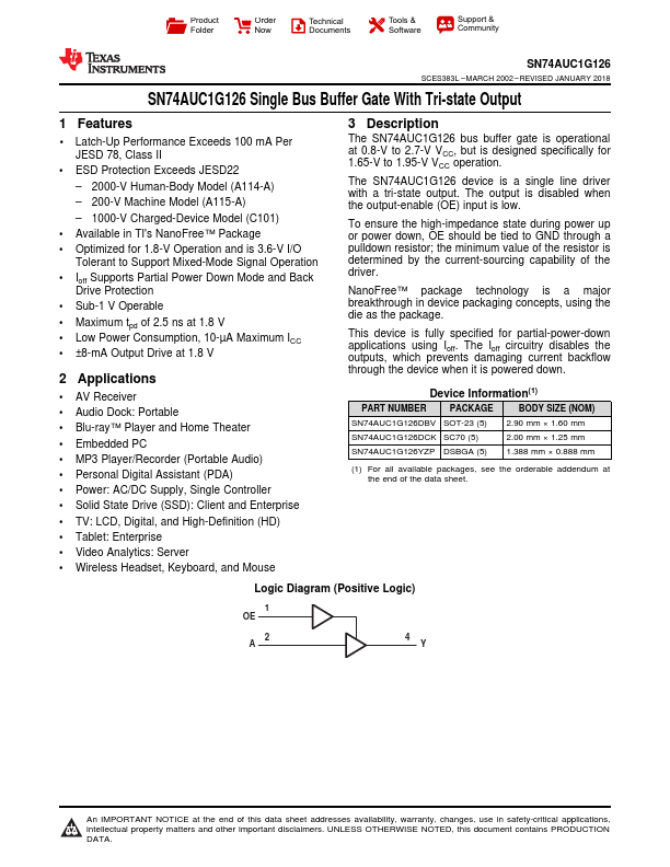
The SN74AUC1G126 bus buffer gate is operational at 0.8-V to 2.7-V VCC, but is designed specifically for 1.65-V to 1.95-V VCC operation.
The SN74AUC1G126 device is a single line driver with a tri-state output.
The output is disabled when the output-enable (OE) input is low.
| Part number | SN74AUC1G126 |
|---|---|
| Manufacturer | Texas Instruments |
| File Size | 1.39 MB |
| Description | Single Bus Buffer Gate |
| Datasheet |
SN74AUC1G126 Datasheet
|
|
|
|
| Part Number | Description | Manufacturer |
|---|---|---|
| SN74101 | AND-OR Gate | ETC |
| SN74102 | AND Gate | ETC |
| SN74103 | Dual J-K Flip-Flop | ETC |
| SN74106 | Dual J-K Flip-Flop | ETC |
| SN74108 | Dual J-K Flip Flop | ETC |
| Part Number | Description |
|---|---|
| SN74AUC1G125 | Single Bus Buffer Gate |
| SN74AUC1G125-EP | Single Bus Buffer Gate |
| SN74AUC1G14 | Single Schmitt-Trigger Inverter |
| SN74AUC1G14-EP | Single Schmitt-Trigger Inverter |
| SN74AUC1G17 | Single Schmitt-Trigger Buffer |
The following content is an automatically extracted verbatim text from the original manufacturer datasheet and is provided for reference purposes only.