CDCLVD2104 Description
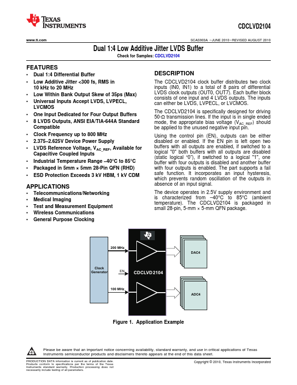
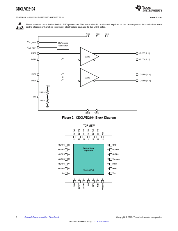
The CDCLVD2104 clock buffer distributes two clock inputs (IN0, IN1) to a total of 8 pairs of differential LVDS clock outputs (OUT0, OUT7). Each buffer block consists of one input and 4 LVDS outputs. The inputs can either be LVDS, LVPECL, or LVCMOS.
CDCLVD2104 Key Features
- Dual 1:4 Differential Buffer
- Low Within Bank Output Skew of 35ps (Max)
- Universal Inputs Accept LVDS, LVPECL
- One Input Dedicated for Four Output Buffers
- 8 LVDS Outputs, ANSI EIA/TIA-644A Standard
- Clock Frequency up to 800 MHz
- 2.375-2.625V Device Power Supply
- Industrial Temperature Range -40°C to 85°C
- Packaged in 5mm × 5mm 28-Pin QFN (RHD)
- ESD Protection Exceeds 3 kV HBM, 1 kV CDM