PLZ30D Overview
Key Specifications
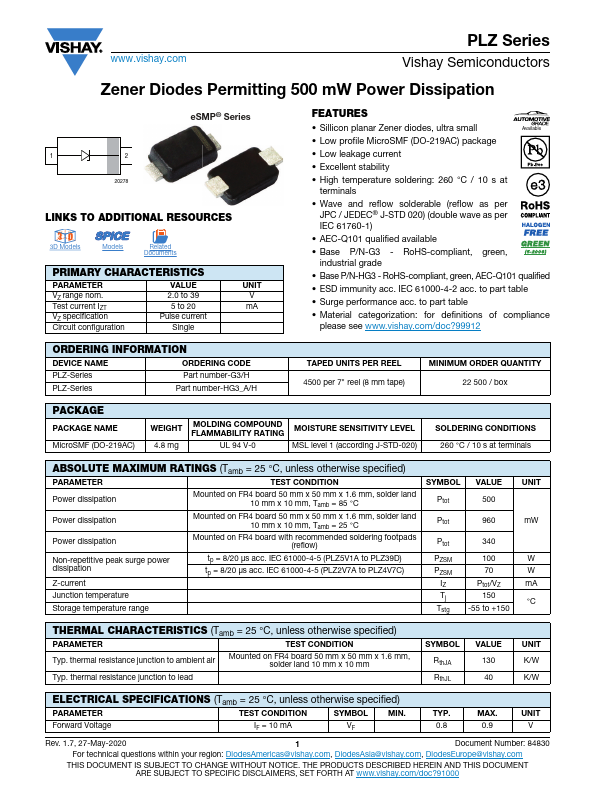
Mount Type: Surface Mount
Max Operating Temp: 150 °C
Key Features
- Sillicon planar Zener diodes, ultra small Available
- Low profile MicroSMF (DO-219AC) package
- Low leakage current
- Excellent stability
- High temperature soldering: 260 °C / 10 s at terminals
- Wave and reflow solderable (reflow as per JPC / JEDEC® J-STD
- (double wave as per IEC 61760-1)
- AEC-Q101 qualified available
- Base P/N-G3 - RoHS-compliant, green, industrial grade
- Base P/N-HG3 - RoHS-compliant, green, AEC-Q101 qualified