The following content is an automatically extracted verbatim text
from the original manufacturer datasheet and is provided for reference purposes only.
View original datasheet text
P8010BIS
N-Channel Enhancement Mode MOSFET
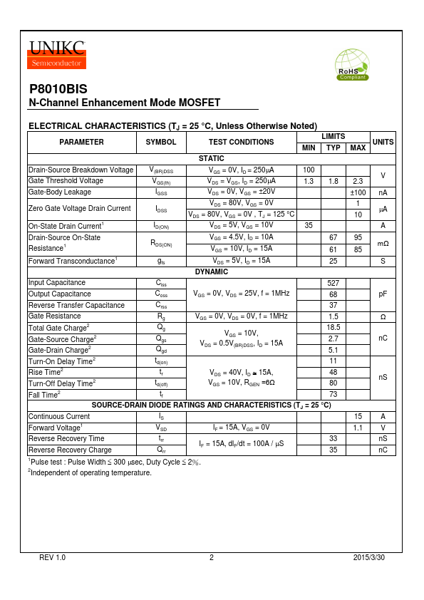
PRODUCT SUMMARY
V(BR)DSS
RDS(ON)
100V
85mΩ @VGS = 10V
ID 15A
TO-251(IS)
1.GATE 2.DRAIN 3.SOURCE
ABSOLUTE MAXIMUM RATINGS (TA = 25 °C Unless Otherwise Noted)
PARAMETERS/TEST CONDITIONS
SYMBOL
LIMITS
Drain-Source Voltage
VDS 100
Gate-Source Voltage
VGS ±20
Continuous Drain Current Pulsed Drain Current1
TC = 25 °C TC = 100 °C
ID IDM
15 9 35
Avalanche Current
IAS 12
Avalanche Energy
L = 0.1mH
EAS
7.2
Power Dissipation
TC = 25 °C TC = 100 °C
PD
46 18
Junction & Storage Temperature Range
TJ, TSTG
-55 to 150
UNITS V
A
mJ W °C
THERMAL RESISTANCE RATINGS
THERMAL RESISTANCE Junction-to-Case 1Pulse width limited by maximum junction temperature.
SYMBOL RqJC
TYPICAL MAXIMUM UNITS 2.7 °C / W
REV 1.
 P8010BIS Datasheet