Datasheet4U Logo Datasheet4U.com
Toshiba logo

TH50VSF3582AASB Datasheet

Manufacturer: Toshiba
TH50VSF3582AASB datasheet preview

TH50VSF3582AASB Details

Part number TH50VSF3582AASB
Datasheet TH50VSF3582AASB_ToshibaSemiconductor.pdf
File Size 611.07 KB
Manufacturer Toshiba
Description MULTI-CHIP INTEGRATED CIRCUIT SILICON GATE CMOS
TH50VSF3582AASB page 2 TH50VSF3582AASB page 3

TH50VSF3582AASB Overview

The TH50VSF3582/3583AASB is a mixed multi-chip package containing a 8,388,608-bit Full CMOS SRAM and a 33,554,432-bit flash memory. The CIOS and CIOF inputs can be used to select the optimal memory configuration. FLASH MEMORY a Simultaneous Read/Write operation so that data can be read during a Write or Erase operation.

TH50VSF3582AASB Key Features

  • Data retention supply voltage VCCs = 1.5 V~3.3 V
  • Current consumption Operating: 45 mA maximum (CMOS level) Standby: 10 µA maximum (SRAM CMOS level) Standby: 10 µA maximu
  • Block erase architecture for flash memory 8 × 8 Kbytes 63 × 64 Kbytes
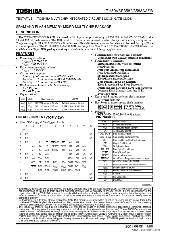
  • Organization
  • PIN ASSIGNMENT (TOP VIEW)
  • Case: CIOF = VCC, CIOS = VCC (×16, ×16)
  • TOSHIBA is continually working to improve the quality and reliability of its products. Nevertheless, semiconductor devic

TH50VSF3582AASB Distributor

Toshiba Datasheets

More from Toshiba

Datasheet4U Logo
Since 2006. D4U Semicon. About Datasheet4U Contact Us Privacy Policy Purchase of parts