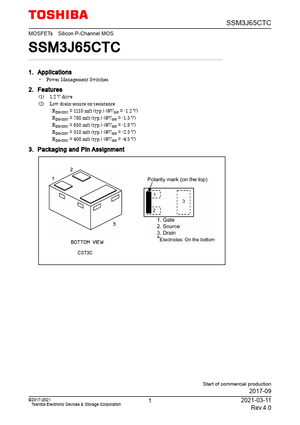
Features
(1) 1.2 V drive (2) Low drain-source on-resistance
: RDS(ON) = 1110 mΩ (typ. ) (@VGS = -1.2 V) RDS(ON) = 780 mΩ (typ. ) (@VGS = -1.5 V) RDS(ON) = 650 mΩ (typ. ) (@VGS = -1.8 V) RDS(ON) = 510 mΩ (typ. ) (@VGS = -2.5 V) RDS(ON) = 400 mΩ (typ. ) (@VGS = -4.5 V)
3. Packaging and Pin Assignment
SSM3J65CTC
CST3C
©2017-2021
1
Toshiba Electronic Devices & Storage Corporation
Start of commercial production
2017-09
2021-03-11 Rev.4.0
SSM3J65CTC
4. Absolute Maximum Ratings (Note) (Unless otherwise speci.
📁 Similar Datasheet
Part Number
Description
Manufacturer
SSM3J01F
Silicon P-Channel MOSFET
Toshiba Semiconductor
SSM3J01T
TOSHIBA Field Effect Transistor Silicon P Channel MOS Type
Toshiba Semiconductor
SSM3J02F
TOSHIBA Field Effect Transistor Silicon P Channel MOS Type
Toshiba Semiconductor
SSM3J02T
TOSHIBA Field Effect Transistor Silicon P Channel MOS Type
Toshiba Semiconductor
SSM3J05FU
Power Management Switch High Speed Switching Applications
Toshiba Semiconductor
Other Datasheets by Toshiba
Full PDF Text Transcription (Reference)
The following content is an automatically extracted verbatim text
from the original manufacturer datasheet and is provided for reference purposes only.
View original datasheet text
MOSFETs Silicon P-Channel MOS
SSM3J65CTC
1. Applications
• Power Management Switches
2. Features
(1) 1.2 V drive (2) Low drain-source on-resistance
: RDS(ON) = 1110 mΩ (typ.) (@VGS = -1.2 V) RDS(ON) = 780 mΩ (typ.) (@VGS = -1.5 V) RDS(ON) = 650 mΩ (typ.) (@VGS = -1.8 V) RDS(ON) = 510 mΩ (typ.) (@VGS = -2.5 V) RDS(ON) = 400 mΩ (typ.) (@VGS = -4.5 V)
3. Packaging and Pin Assignment
SSM3J65CTC
CST3C
©2017-2021
1
Toshiba Electronic Devices & Storage Corporation
Start of commercial production
2017-09
2021-03-11 Rev.4.0
SSM3J65CTC
4.
Published:
Jun 22, 2019
|
 SSM3J65CTC Datasheet