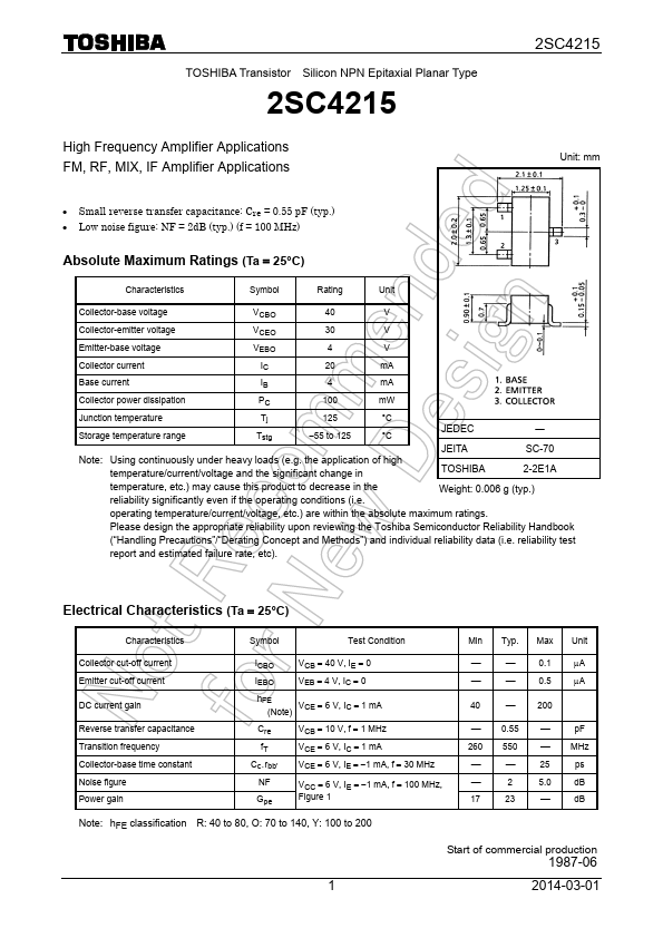
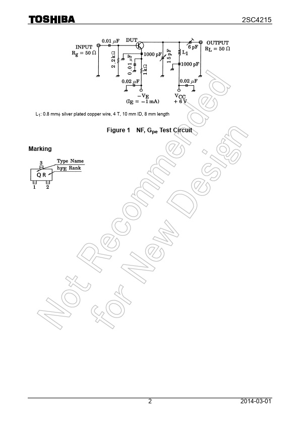
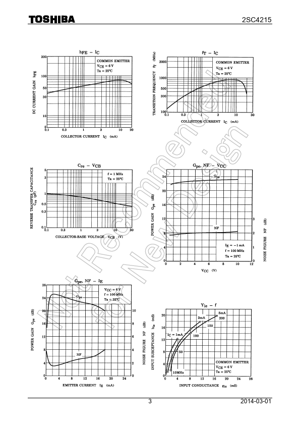
TOSHIBA Transistor Silicon NPN Epitaxial Planar Type
2SC4215
High Frequency Amplifier Applications
FM, RF, MIX, IF Amplifier Applications
2SC4215
Unit: mm
• Small reverse transfer capacitance: Cre = 0.55 pF (typ.)
• Low noise figure: NF = 2dB (typ.) (f = 100 MHz)
Absolute Maximum Ratings (Ta = 25°C)
Characteristics
Symbol
Rating
Unit
Collector-base voltage
VCBO 40 V
Collector-emitter voltage
VCEO 30 V
Emitter-base voltage
VEBO 4 V
Collector current
IC 20 mA
Base current
IB 4 mA
Collector power dissipation
PC 100 mW
Junction temperature
Storage temperature range
Tj 125 °C
Tstg
−55~125
°C
JEDEC
―
Note: Using continuously under heavy loads (e.g. the application of high
temperature/current/voltage and the significant change in
JEITA
TOSHIBA
SC-70
2-2E1A
temperature, etc.) may cause this product to decrease in the
reliability significantly even if the operating conditions (i.e.
Weight: 0.006 g (typ.)
operating temperature/current/voltage, etc.) are within the absolute maximum ratings.
Please design the appropriate reliability upon reviewing the Toshiba Semiconductor Reliability Handbook
(“Handling Precautions”/“Derating Concept and Methods”) and individual reliability data (i.e. reliability test
report and estimated failure rate, etc).
Electrical Characteristics (Ta = 25°C)
Characteristics
Symbol
Test Condition
Collector cut-off current
Emitter cut-off current
DC current gain
Reverse transfer capacitance
Transition frequency
Collector-base time constant
Noise figure
Power gain
ICBO
VCB = 40 V, IE = 0
IEBO
VEB = 4 V, IC = 0
hFE
(Note)
VCE = 6 V, IC = 1 mA
Cre
fT
Cc・rbb’
NF
Gpe
VCB = 10 V, f = 1 MHz
VCE = 6 V, IC = 1 mA
VCE = 6 V, IE = −1 mA, f = 30 MHz
VCC = 6 V, IE = −1 mA, f = 100 MHz,
Figure 1
Note: hFE classification R: 40~80, O: 70~140, Y: 100~200
Min Typ. Max Unit
⎯ ⎯ 0.1 μA
⎯ ⎯ 0.5 μA
40 ⎯ 200
⎯ 0.55 ⎯
pF
260 550 ⎯ MHz
⎯ ⎯ 25 ps
⎯ 2 5.0 dB
17 23 ⎯ dB
1 2007-11-01