Datasheet Details
| Part number | SI53366 |
|---|---|
| Manufacturer | Silicon Laboratories |
| File Size | 6.26 MB |
| Description | LVCMOS Fanout Clock Buffers |
| Datasheet |
 SI53366 Datasheet SI53366 Datasheet
|
|
|
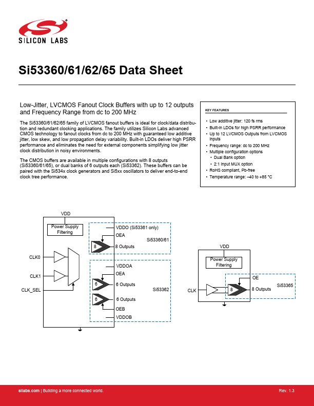
Download the SI53366 datasheet PDF. This datasheet also covers the SI53360 variant, as both devices belong to the same lvcmos fanout clock buffers family and are provided as variant models within a single manufacturer datasheet.
.
.
.
4 2.2 Input Mux.
.
.
.
.
| Part number | SI53366 |
|---|---|
| Manufacturer | Silicon Laboratories |
| File Size | 6.26 MB |
| Description | LVCMOS Fanout Clock Buffers |
| Datasheet |
SI53366 Datasheet
|
|
|
|
| Part Number | Description | Manufacturer |
|---|---|---|
| Si53360 | LVCMOS Fanout Clock Buffers | Skyworks |
| Si53361 | LVCMOS Fanout Clock Buffers | Skyworks |
| Si53362 | LVCMOS Fanout Clock Buffers | Skyworks |
| Si53365 | LVCMOS Fanout Clock Buffers | Skyworks |
| Si53301 | Ultra-Low Additive Jitter Fanout Clock Buffers | Skyworks |
| Part Number | Description |
|---|---|
| SI53360 | LVCMOS Fanout Clock Buffers |
| SI53361 | LVCMOS Fanout Clock Buffers |
| SI53362 | LVCMOS Fanout Clock Buffers |
| SI53365 | 1:8 LOW JITTER CMOS CLOCK BUFFER |
| SI533 | DUAL FREQUENCY CRYSTAL OSCILLATOR |
The following content is an automatically extracted verbatim text from the original manufacturer datasheet and is provided for reference purposes only.