Click to expand full text
Ordering number : EN*A1229A
CMOS IC
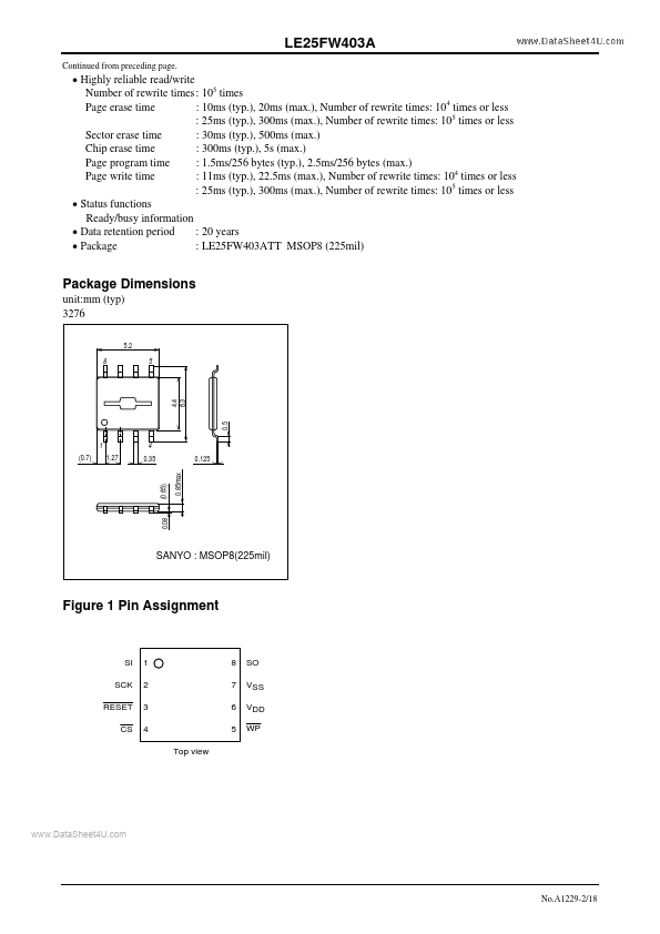
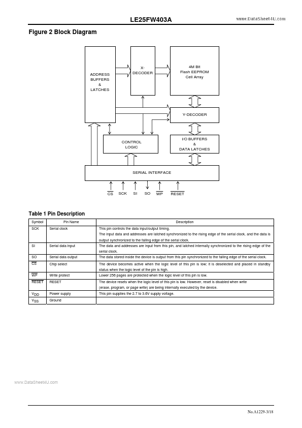
LE25FW403A
Overview
4M-bit (512K×8) Serial Flash Memory 30MHz SPI Bus
The LE25FW403A is an onboard programmable flash memory device with a 512K×8-bit configuration. It uses a single 3.0V power supply and supports the serial interface. It has three erase functions depending on the size of memory area in which the data is to be erased: the chip erase function, the sector (64K bytes) erase function, and a page (256 bytes) erase function. A page program method is supported for data writing and it can program any amount of data from 1 to 256 bytes. The page program time depends on the number of bytes programmed and the IC provides a high-speed program time of 1.5ms (typ) when programming 256 bytes at one time.
 LE25FW403A Datasheet