SDM4435
SDM4435 is P-Channel Enhancement Mode MOS FET manufactured by SamHop.
S DM4435
P -C hannel E nhancement Mode MOS FE T
J ul.27 2004 ver1.1
P R ODUC T S UMMAR Y
V DS S ID R DS (ON) ( m W ) Max
-30V
-8A
20 @ VGS = -10V 35 @ VGS = -4.5V
F E AT UR E S S uper high dense cell design for low R DS(ON).
R ugged and reliable. S urface Mount P ackage.
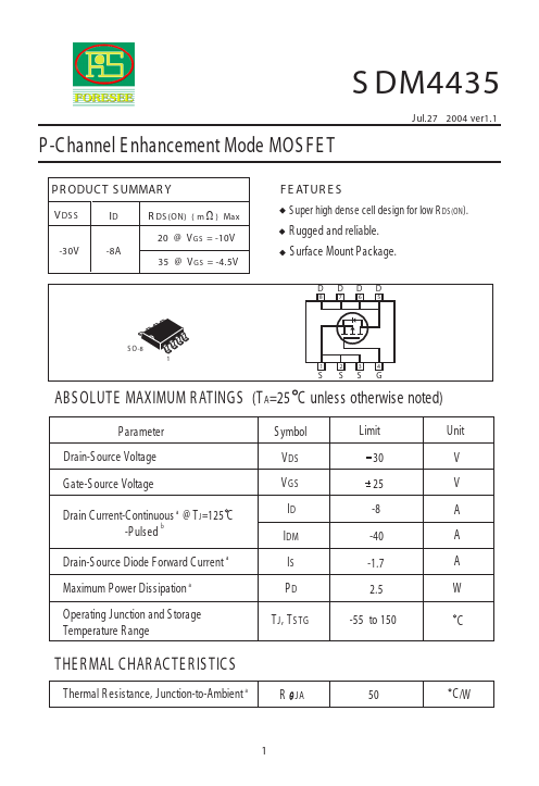
DDDD
8 7 65
S O-8
1 234
S SS G
ABS OLUTE MAXIMUM R ATINGS (TA=25 C unless otherwise noted)
P arameter Drain-S ource Voltage Gate-S ource Voltage
Drain C urrent-C ontinuous a @ TJ=125 C -P ulsed b
Drain-S ource Diode Forward C urrent a Maximum P ower Dissipation a Operating Junction and S torage Temperature R ange
S ymbol VDS VGS ID IDM IS PD
TJ, TSTG
Limit 30 25 -8 -40 -1.7 2.5
-55 to 150
Unit V V A A...