The following content is an automatically extracted verbatim text
from the original manufacturer datasheet and is provided for reference purposes only.
View original datasheet text
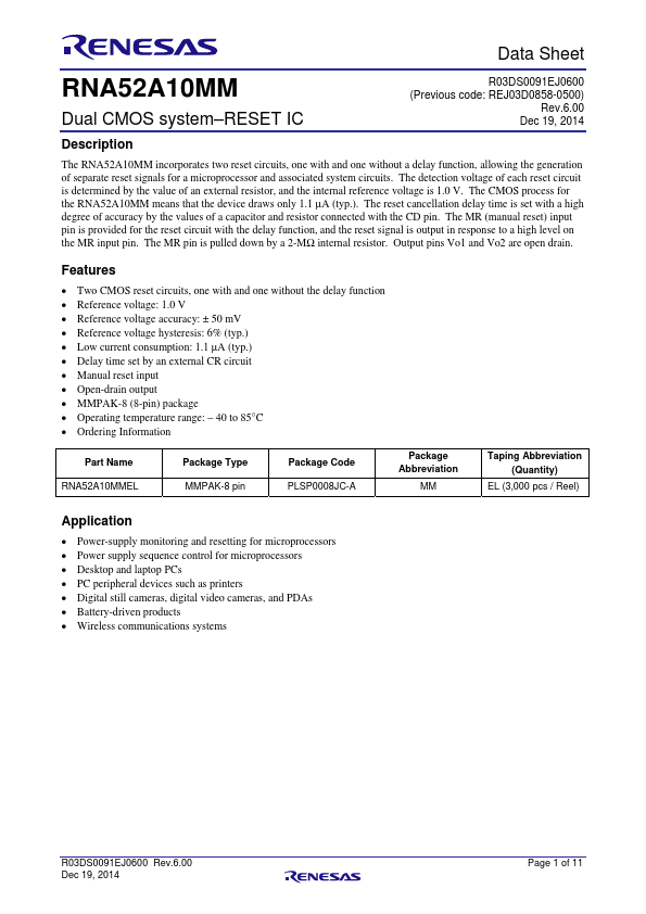
Data Sheet
RNA52A10MM
Dual CMOS system–RESET IC
R03DS0091EJ0600 (Previous code: REJ03D0858-0500)
Rev.6.00 Dec 19, 2014
Description
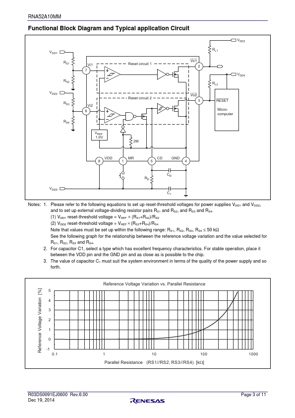
The RNA52A10MM incorporates two reset circuits, one with and one without a delay function, allowing the generation of separate reset signals for a microprocessor and associated system circuits. The detection voltage of each reset circuit is determined by the value of an external resistor, and the internal reference voltage is 1.0 V. The CMOS process for the RNA52A10MM means that the device draws only 1.1 μA (typ.). The reset cancellation delay time is set with a high degree of accuracy by the values of a capacitor and resistor connected with the CD pin.
 RNA52A10MM Datasheet