The RNA52A10T incorporates two reset circuits, one with and one without a delay function, allowing the generation of separate reset signals for a microprocessor and associated system circuits.
Key Features
Two CMOS reset circuits, one with and one without the delay function.
Full PDF Text Transcription for RNA52A10T (Reference)
Note: Below is a high-fidelity text extraction (approx. 800 characters) for
RNA52A10T. For precise diagrams, and layout, please refer to the original PDF.
Data Sheet RNA52A10T Dual CMOS system–RESET IC R03DS0078EJ0200 Rev.2.00 Dec 19, 2015 Description The RNA52A10T incorporates two reset circuits, one with and one without a...
View more extracted text
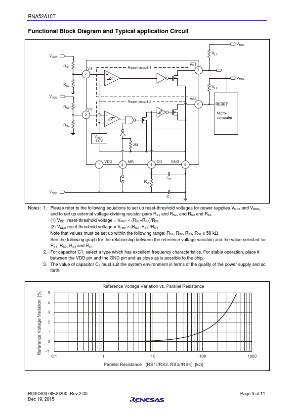
RNA52A10T incorporates two reset circuits, one with and one without a delay function, allowing the generation of separate reset signals for a microprocessor and associated system circuits. The detection voltage of each reset circuit is determined by the value of an external resistor, and the internal reference voltage is 1.0 V. The CMOS process for the RNA52A10T means that the device draws only 1.1 μA (typ.). The reset cancellation delay time is set with a high degree of accuracy by the values of a capacitor and resistor connected with the CD pin.
 RNA52A10T Datasheet