Datasheet4U Logo Datasheet4U.com

HD74LV2GT245A - Dual Bus Transceivers

Description

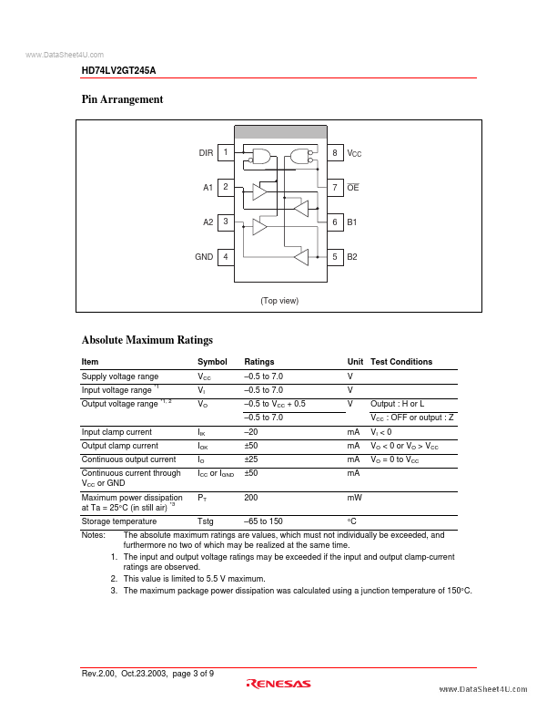
The HD74LV2GT245A has two buffers with three state output in a 8 pin package.

When DIR is high, data is transferred from the A inputs to the B outputs, and when DIR is low, data is transferred from the B inputs to the A outputs.

Features

  • The basic gate function is lined up as Renesas uni logic series.
  • Supplied on emboss taping for high-speed automatic mounting.
  • TTL compatible input level. Supply voltage range : 3.0 to 5.5 V Operating temperature range :.
  • 40 to +85°C.
  • Logic-level translate function 3.0 V CMOS logic → 5.0 V CMOS logic (@VCC = 5.0 V) 1.8 V or 2.5 V CMOS logic → 3.3 V CMOS logic (@VCC = 3.3 V).
  • All inputs VIH (Max. ) = 5.5 V (@VCC = 0 V to 5.5 V) All outputs VO.

📥 Download Datasheet

Datasheet preview – HD74LV2GT245A
Other Datasheets by Renesas Technology

Full PDF Text Transcription

Click to expand full text
www.DataSheet4U.com HD74LV2GT245A Dual Bus Transceivers with 3–state Outputs / CMOS Logic Level Shifter REJ03D0153–0200Z (Previous ADE-205-694A (Z)) Rev.2.00 Oct.23.2003 Description The HD74LV2GT245A has two buffers with three state output in a 8 pin package. When DIR is high, data is transferred from the A inputs to the B outputs, and when DIR is low, data is transferred from the B inputs to the A outputs. The A and B buses are separated by making the enable input (OE) high level. The input protection circuitry on this device allows over voltage tolerance on the input, allowing the device to be used as a logic–level translator from 3.0 V CMOS Logic to 5.0 V CMOS Logic or from 1.8 V CMOS logic to 3.0 V CMOS Logic while operating at the high-voltage power supply.
Published: |