Click to expand full text
www.DataSheet4U.com
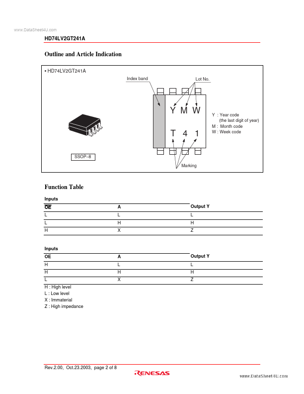
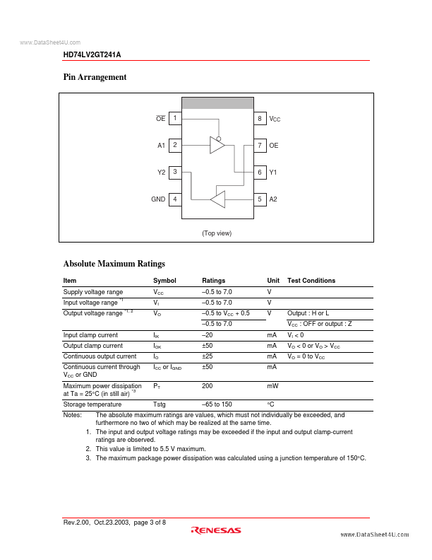
HD74LV2GT241A
Dual Bus Buffer Noninverted with 3–state Output / CMOS Logic Level Shifter
REJ03D0152–0200Z (Previous ADE-205-679A (Z)) Rev.2.00 Oct.23.2003
Description
The HD74LV2GT241A has dual bus buffer noninverted with 3–state output in an 8 pin package. Two noninverters are included in one circuit. Each circuit can be independently controlled by the enable signal OE or OE, which enables outputs when receiving a low or high-level signal, respectively. The input protection circuitry on this device allows over voltage tolerance on the input, allowing the device to be used as a logic–level translator from 3.0 V CMOS Logic to 5.0 V CMOS Logic or from 1.8 V CMOS logic to 3.0 V CMOS Logic while operating at the high-voltage power supply.
 HD74LV2GT241A Datasheet