MPC9893 Datasheet Text
3.3V 1:12 LVCMOS PLL Clock Generator
MPC9893
PRODUCT DISCONTINUATION NOTICE
- LAST TIME BUY EXPIRES SEPTEMBER 7, 2016
DATASHEET
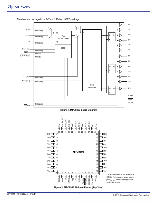
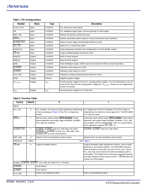
The MPC9893 is a 2.5 V and 3.3 V patible, PLL based intelligent dynamic clock switch and generator specifically designed for redundant clock distribution systems. The device receives two LVCMOS clock signals and generates 12 phase aligned output clocks. The MPC9893 is able to detect a failing reference clock signal and to dynamically switch to a redundant clock signal. The switch from the failing clock to the redundant clock occurs without interruption of the output clock signal (output clock slews to alignment). The phase bump typically caused by a clock failure is eliminated.
The device offers 12 low skew clock outputs organized into two output banks, each configurable to support the different clock frequencies.
The extended temperature range of the MPC9893 supports telemunication and networking requirements. The device employs a fully differential PLL design to minimize jitter.
Features
- 12-output LVCMOS PLL clock generator
- 2.5 V and 3.3 V patible
- IDCS
- on-chip intelligent dynamic clock switch
- Automatically detects clock failure
- Smooth output phase transition during clock failover switch
- 7.5
- 200 MHz output frequency range
- LVCMOS patible inputs and outputs
- External feedback enables zero-delay configurations
- Supports networking, telemunications and puter applications
- Output enable/disable and static test mode (PLL bypass)
- Low skew characteristics: maximum 50 ps output-to-output (within bank)
- 48-lead LQFP package, Pb-free
- Ambient operating temperature range of -40 to 85C
- For functional replacement use 87973
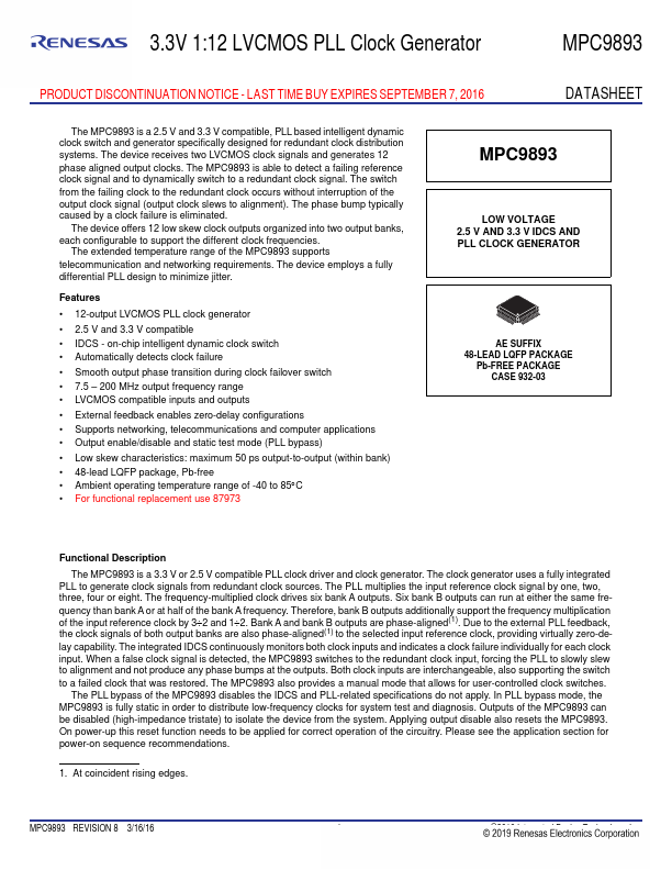
MPC9893
LOW VOLTAGE 2.5 V AND 3.3 V IDCS AND PLL CLOCK GENERATOR
SCALE 2:1
AE...