ISL3296E
Key Features
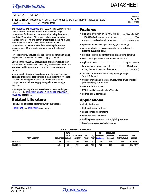
- ISL3295E and ISL3298E device pages Features
- Specified for +125°C operation (VCC ≤ 3.6V only)
- Logic supply pin (VL) eases operation in mixed supply systems (ISL3298E only)
- Hot plug - Tx outputs remain three-state during power-up
- Low Tx leakage allows >256 devices on the bus
- -7V to +12V common-mode output voltage range (VCC ≤ 3.6V only)
- Current limiting and thermal shutdown for driver overload protection (VCC ≤ 3.6V only)
- Tri-statable Tx outputs
- 5V tolerant logic inputs when VCC ≤5V
- Pb-free (RoHS compliant)