8S89832I Overview
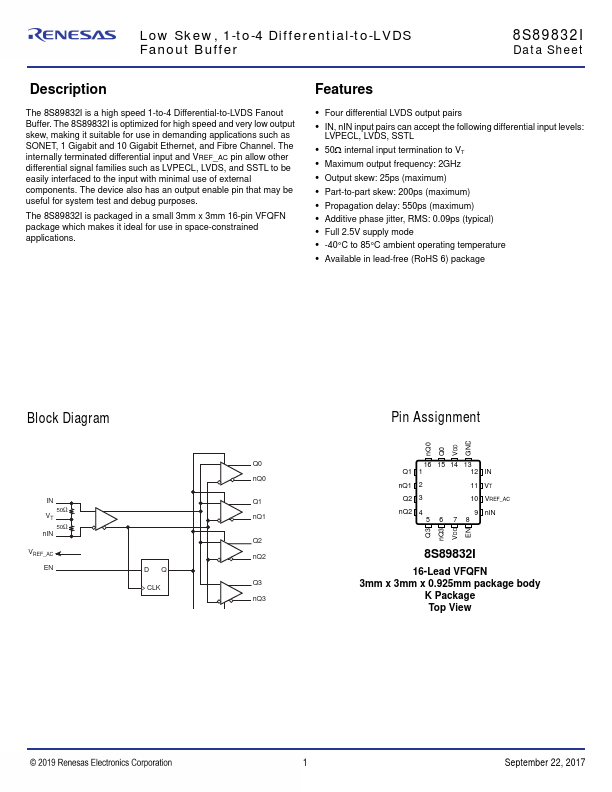
The 8S89832I is a high speed 1-to-4 Differential-to-LVDS Fanout Buffer. The 8S89832I is optimized for high speed and very low output skew, making it suitable for use in demanding applications such as SONET, 1 Gigabit and 10 Gigabit Ethernet, and Fibre Channel. The internally terminated differential input and VREF_AC pin allow other differential signal families such as LVPECL, LVDS, and SSTL to be easily interfaced...
8S89832I Key Features
- Four differential LVDS output pairs
- IN, nIN input pairs can accept the following differential input levels
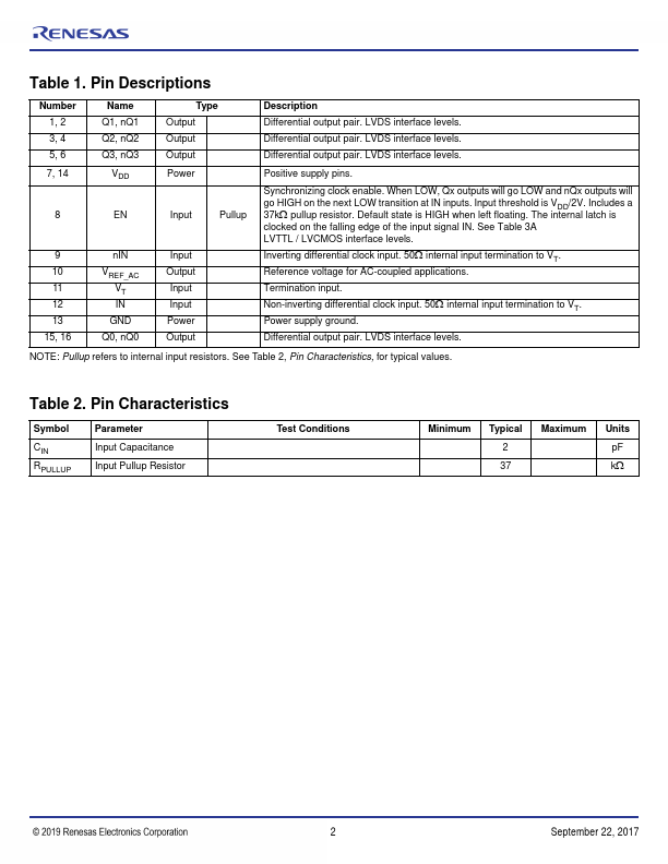
- 50 internal input termination to VT
- Maximum output frequency: 2GHz
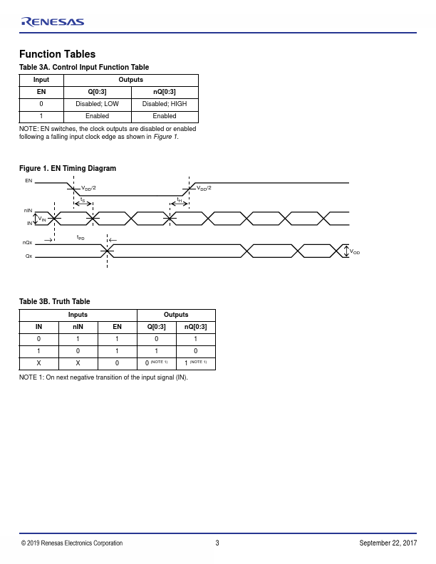
- Output skew: 25ps (maximum)
- Part-to-part skew: 200ps (maximum)
- Propagation delay: 550ps (maximum)
- Additive phase jitter, RMS: 0.09ps (typical)
- Full 2.5V supply mode
- 40°C to 85°C ambient operating temperature