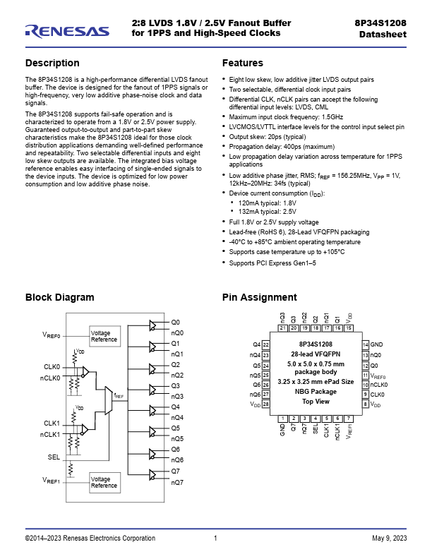
Datasheet4U Logo Datasheet4U.com

8P34S1208 - 2:8 LVDS 1.8V / 2.5V Fanout Buffer

Datasheet Summary

Description

The 8P34S1208 is a high-performance differential LVDS fanout buffer.

The device is designed for the fanout of 1PPS signals or high-frequency, very low additive phase-noise clock and data signals.

Features

  • Eight low skew, low additive jitter LVDS output pairs.
  • Two selectable, differential clock input pairs.
  • Differential CLK, nCLK pairs can accept the following differential input levels: LVDS, CML.
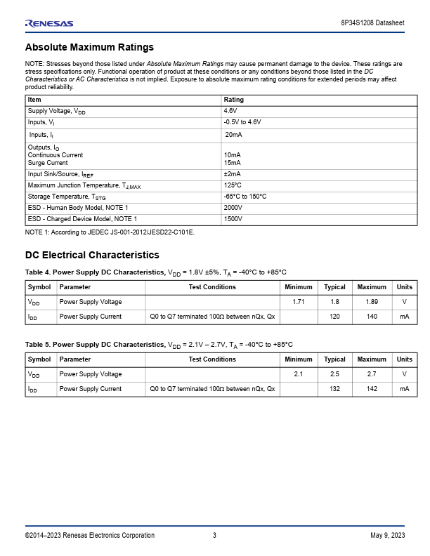
  • Maximum input clock frequency: 1.5GHz.
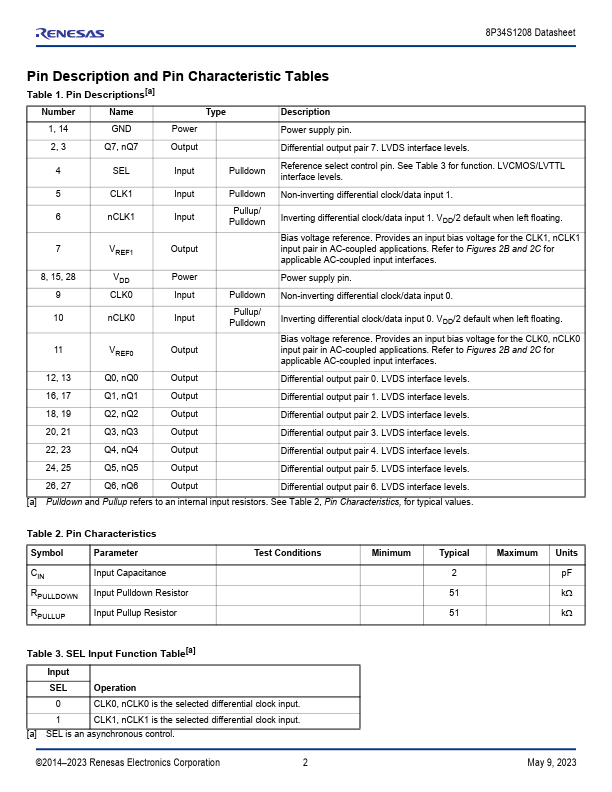
  • LVCMOS/LVTTL interface levels for the control input select pin.
  • Output skew: 20ps (typical).
  • Propagation delay: 400ps (maximum).
  • Low propagation delay variation across temperature for 1PPS appl.

📥 Download Datasheet

Datasheet preview – 8P34S1208

Datasheet Details

Part number 8P34S1208
Manufacturer Renesas
File Size 1.26 MB
Description 2:8 LVDS 1.8V / 2.5V Fanout Buffer
Datasheet download datasheet 8P34S1208 Datasheet
Additional preview pages of the 8P34S1208 datasheet.
Other Datasheets by Renesas

Full PDF Text Transcription

Click to expand full text
2:8 LVDS 1.8V / 2.5V Fanout Buffer for 1PPS and High-Speed Clocks 8P34S1208 Datasheet Description The 8P34S1208 is a high-performance differential LVDS fanout buffer. The device is designed for the fanout of 1PPS signals or high-frequency, very low additive phase-noise clock and data signals. The 8P34S1208 supports fail-safe operation and is characterized to operate from a 1.8V or 2.5V power supply. Guaranteed output-to-output and part-to-part skew characteristics make the 8P34S1208 ideal for those clock distribution applications demanding well-defined performance and repeatability. Two selectable differential inputs and eight low skew outputs are available. The integrated bias voltage reference enables easy interfacing of single-ended signals to the device inputs.
Published: |