Datasheet Details
| Part number | 8P34S1102 |
|---|---|
| Manufacturer | Renesas |
| File Size | 1.34 MB |
| Description | 1:2 LVDS 1.8V / 2.5V Fanout Buffer |
| Datasheet |
 8P34S1102 Datasheet 8P34S1102 Datasheet
|
|
|
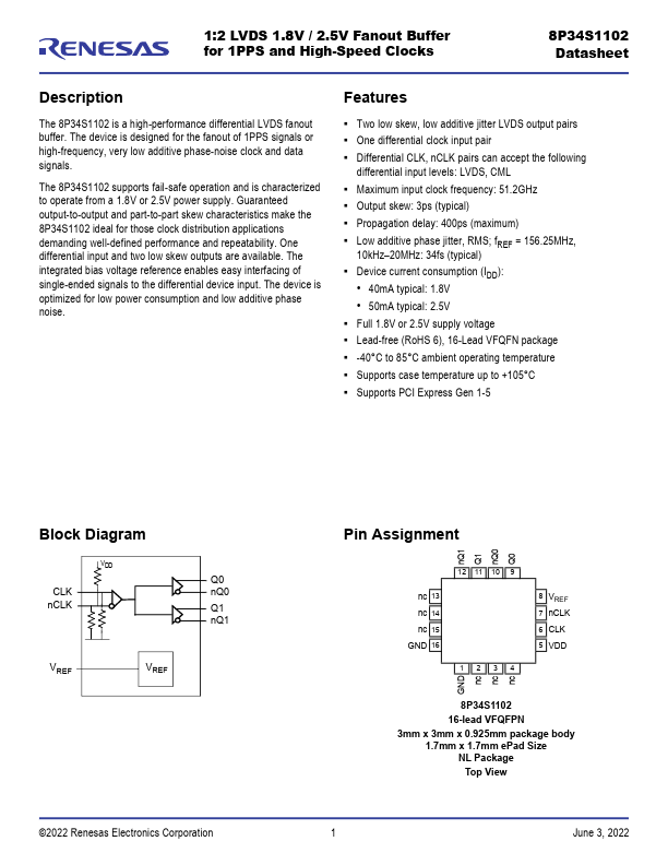
The 8P34S1102 is a high-performance differential LVDS fanout buffer.
The device is designed for the fanout of 1PPS signals or high-frequency, very low additive phase-noise clock and data signals.
| Part number | 8P34S1102 |
|---|---|
| Manufacturer | Renesas |
| File Size | 1.34 MB |
| Description | 1:2 LVDS 1.8V / 2.5V Fanout Buffer |
| Datasheet |
8P34S1102 Datasheet
|
|
|
|