8205A
8205A is Dual N-Channel MOSFET manufactured by RZC Microelectronics.
DESCRIPTION
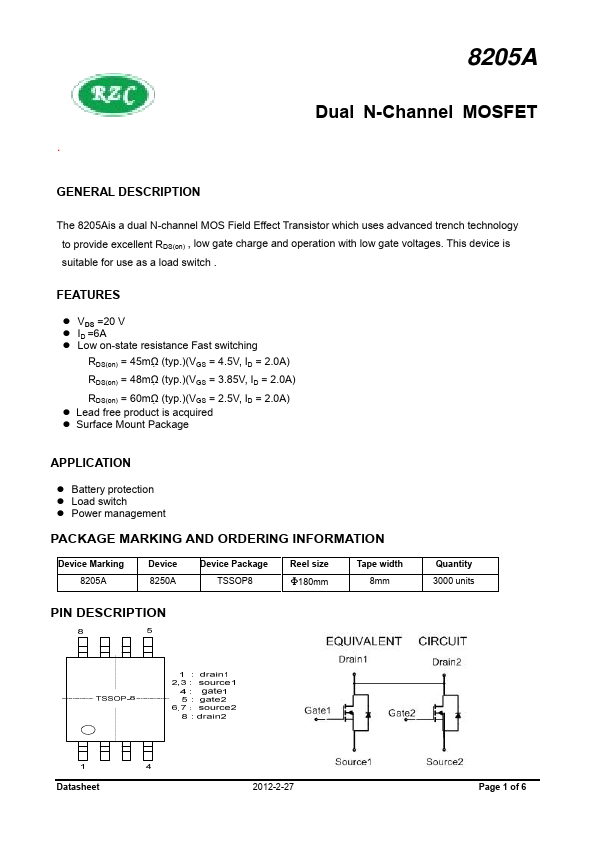
The 8205Ais a dual N-channel MOS Field Effect Transistor which uses advanced trench technology to provide excellent RDS(on) , low gate charge and operation with low gate voltages. This device is suitable for use as a load switch .
Features l VDS =20 V l ID =6A l Low on-state resistance Fast switching RDS(on) = 45mΩ (typ.)(VGS = 4.5V, ID = 2.0A) RDS(on) = 48mΩ (typ.)(VGS = 3.85V, ID = 2.0A) RDS(on) = 60mΩ (typ.)(VGS = 2.5V, ID = 2.0A) l Lead free product is acquired l Surface Mount Package
APPLICATION l Battery protection l Load switch l Power management
PACKAGE MARKING AND ORDERING INFORMATION
Device Marking 8205A Device 8250A Device Package TSSOP8 Reel size Tape width 8mm Quantity 3000 units
Φ180mm
PIN DESCRIPTION
2012-2-27
Page 1 of 6
PIN NUM 1 2 3 4 5 6 7 8 PIN NAME D S1 S1 G1 G2 S2 S2 D PIN FUNCTION DRAIN SOURCE1 SOURCE1 GATE2 GATE2 SOURCE2 SOURCE2 DRAIN
ABSOLUTE MAXIMUM RATINGS (TA = 25℃)
Symbol VDS ID IDM VGS PD
Tstg
Parameter Drain-source Voltage Drain Current(continuous)at Tc=25℃ Drain Current (pulsed) Gate-source Voltage Power Dissipation (TC = 25°C)
Operating and Storage Temperature Rang
Value 20 (Note1) (Note2) (Note1) 6 24 ±12 1.25
-55 to +150
Unit V A A V W
℃
Notes a. PW<10us,Duty Cycle<1%,VGS=4.5V 2 b. Mounted on ceramic substrate of 45 cm x 2.2mm. Caution: These values must not be exceeded under any conditions. Remark: The diode connected between the gate and source of the transistor serves as a protector against ESD. When this device actually used, an additional protection circuit is externally required if a voltage exceeding the rated voltage may be applied to this device.
Thermal Data
Symbol Rthj-amb Parameter Thermal Resistance Junction- ambient Max. 83 Unit ℃/W
Electrical Characteristics (TC = 25℃)
Symbol V(BR)DSS IDSS IGSS VGS(th) Parameter Drain-source Breakdown Voltage Zero Gate Voltage Drain Current Gate Leakage Current Gate threshold voltage Test Conditions ID=250u A, VGS=0V VDS=20V,VGS=0V...