Datasheet Details
| Part number | SN74LS174 |
|---|---|
| Manufacturer | onsemi |
| File Size | 178.06 KB |
| Description | Hex D Flip-Flop |
| Datasheet |
 SN74LS174 Datasheet SN74LS174 Datasheet
|

|
|
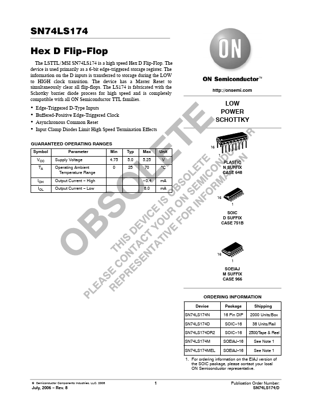
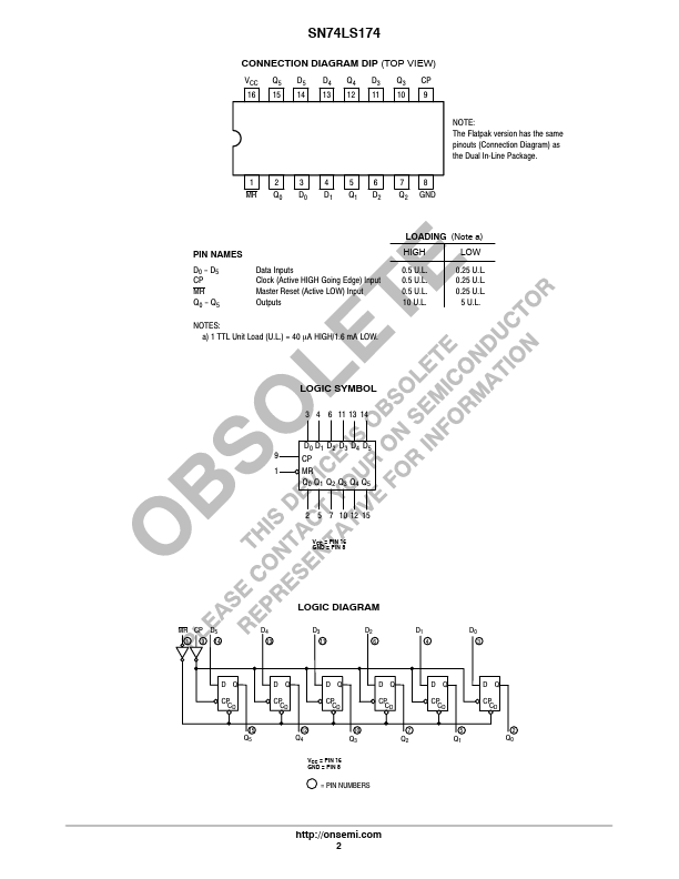
The LS174 consists of six edge-triggered D flip-flops with individual D inputs and Q outputs.
The Clock (CP) and Master Reset (MR) are common to all flip-flops.
Each D input’s state is transferred to the corresponding flip-flop’s output following the LOW to HIGH Clock (CP) transition.
| Part number | SN74LS174 |
|---|---|
| Manufacturer | onsemi |
| File Size | 178.06 KB |
| Description | Hex D Flip-Flop |
| Datasheet |
SN74LS174 Datasheet
|
|
|
|
| Part Number | Description | Manufacturer |
|---|---|---|
| SN74LS174 | HEX D FLIP-FLOP | Motorola |
| SN74LS174 | HEX/QUADRUPLE D-TYPE FLIP-FLOPS | Texas Instruments |
| SN74LS170 | 4 x 4 REGISTER FILE OPEN-COLLECTOR | Motorola |
| SN74LS171 | QUADRUPLE D-TYPE FLIP-FLOPS | Texas Instruments |
| SN74LS173A | 4-BIT D-TYPE REGISTER | Motorola |
| Part Number | Description |
|---|---|
| SN74LS175 | Quad D Flip-Flop |
| SN74LS10 | TRIPLE 3-INPUT NAND GATE |
| SN74LS109 | LOW POWER SCHOTTKY |
| SN74LS109A | Dual JK Positive Edge-Triggered Flip-Flop |
| SN74LS122 | Retriggerable Monostable Multivibrator |
The following content is an automatically extracted verbatim text from the original manufacturer datasheet and is provided for reference purposes only.