Click to expand full text
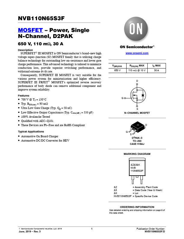
NVB110N65S3F
MOSFET – Power, Single N-Channel, D2PAK
650 V, 110 mW, 30 A
Description SUPERFET® III MOSFET is ON Semiconductor’s brand−new high
voltage super−junction (SJ) MOSFET family that is utilizing charge balance technology for outstanding low on−resistance and lower gate charge performance. This advanced technology is tailored to minimize conduction loss, provide superior switching performance, and withstand extreme dv/dt rate.
Consequently, SUPERFET III MOSFET is very suitable for the various power system for miniaturization and higher efficiency. SUPERFET III FRFET® MOSFET’s optimized reverse recovery performance of body diode can remove additional component and improve system reliability.
Features
• 700 V @ TJ = 150°C • Typ. RDS(on) = 93 mW • Ultra Low Gate Charge (Typ.
 NVB110N65S3F Datasheet