NTMFD4C86N
Features
- Co- Packaged Power Stage Solution to Minimize Board Space
- Minimized Parasitic Inductances
- Optimized Devices to Reduce Power Losses
- These Devices are Pb- Free, Halogen Free/BFR Free and are Ro HS pliant
Applications
- DC- DC Converters
- System Voltage Rails
- Point of Load
.onsemi.
V(BR)DSS
Q1 Top FET 30 V
Q2 Bottom FET 30 V
RDS(on) MAX 5.4 m W @ 10 V 8.1 m W @ 4.5 V 2.6 m W @ 10 V 3.4 m W @ 4.5 V
ID MAX 20 A
32 A
D1 (3, 4, 9)
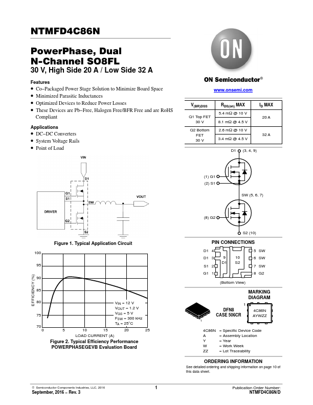
EFFICIENCY (%)
Figure 1. Typical Application Circuit
80 VIN = 12 V VOUT = 1.2 V
75 VGS = 5 V FSW = 300 k Hz
70 TA = 25°C 0 5 10 15 20 25 LOAD CURRENT (A) Figure 2. Typical Efficiency Performance POWERPHASEGEVB Evaluation Board
© Semiconductor ponents Industries, LLC, 2015
July, 2015
- Rev. 1
(1) G1 (2) S1
SW (5, 6, 7)
(8) G2
S2 (10)
PIN CONNECTIONS
D1 4
D1 3 9 10 D1 S2
S1 2
G1 1
5 SW 6 SW 7 SW 8...