Click to expand full text
NTMFD4C85N
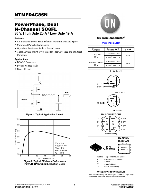
PowerPhase, Dual N-Channel SO8FL
30 V, High Side 25 A / Low Side 49 A
Features
• Co−Packaged Power Stage Solution to Minimize Board Space • Minimized Parasitic Inductances • Optimized Devices to Reduce Power Losses • These Devices are Pb−Free, Halogen Free/BFR Free and are RoHS
Compliant
Applications
• DC−DC Converters • System Voltage Rails • Point of Load
www.onsemi.com
V(BR)DSS
Q1 Top FET 30 V
Q2 Bottom FET 30 V
RDS(ON) MAX 3.0 mW @ 10 V 4.3 mW @ 4.5 V 0.8 mW @ 10 V 1.2 mW @ 4.5 V
ID MAX 25 A
49 A
D1 (3, 4, 9)
EFFICIENCY (%)
Figure 1. Typical Application Circuit
100
95
90
85
80 VIN = 12 V VOUT = 1.2 V
75 VGS = 5 V FSW = 300 kHz
70 TA = 25°C 0 5 10 15 20 25 30 LOAD CURRENT (A) Figure 2.
 NTMFD4C85N Datasheet