NB7L585
NB7L585 is Differential 1:6 LVPECL Clock/Data distribution manufactured by onsemi.
Description
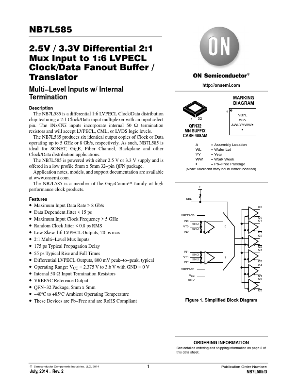
The NB7L585 is a differential 1:6 LVPECL Clock/Data distribution chip featuring a 2:1 Clock/Data input multiplexer with an input select pin. The INx/INx inputs incorporate internal 50 W termination resistors and will accept LVPECL, CML, or LVDS logic levels.
The NB7L585 produces six identical output copies of Clock or Data operating up to 5 GHz or 8 Gb/s, respectively. As such, NB7L585 is ideal for SONET, Gig E, Fiber Channel, Backplane and other Clock/Data distribution applications.
The NB7L585 is powered with either 2.5 V or 3.3 V supply and is offered in a low profile 5mm x 5mm 32- pin QFN package.
Application notes, models, and support documentation are available at .onsemi..
The NB7L585 is a member of the Gigam™ family of high performance clock products.
Features
- Maximum Input Data Rate > 8 Gb/s
- Data Dependent Jitter < 15 ps
- Maximum Input Clock Frequency > 5 GHz
- Random Clock Jitter < 0.8 ps RMS
- Low Skew 1:6 LVPECL Outputs, 20 ps max
- 2:1 Multi- Level Mux Inputs
- 175 ps Typical Propagation Delay
- 55 ps Typical Rise and Fall Times
- Differential LVPECL Outputs, 800 m V peak- to- peak, typical
- Operating Range: VCC = 2.375 V to 3.6 V with GND = 0 V
- Internal 50 W Input Termination Resistors
- VREFAC Reference Output
- QFN- 32 Package, 5mm x 5mm
- - 40ºC to +85ºC Ambient Operating Temperature
- These Devices are Pb- Free and are Ro HS pliant http://onsemi.
MARKING DIAGRAM
1 32
QFN32 MN SUFFIX CASE 488AM
NB7L 585 AWLYYWWG
A = Assembly Location WL = Wafer Lot YY = Year WW = Work Week G = Pb- Free Package (Note: Microdot may be in either location)
+
VREFAC0 IN0 50 W VT0 50 W IN0
Q0
Q0 Q1
Q1 Q2
IN1 50 W
VT1 50...