Datasheet Details
| Part number | NB6L14S |
|---|---|
| Manufacturer | onsemi |
| File Size | 224.77 KB |
| Description | 2.5V 1:4 AnyLevel Differential Input to LVDS Fanout Buffer/Translator |
| Datasheet |
 NB6L14S Datasheet NB6L14S Datasheet
|
|
|
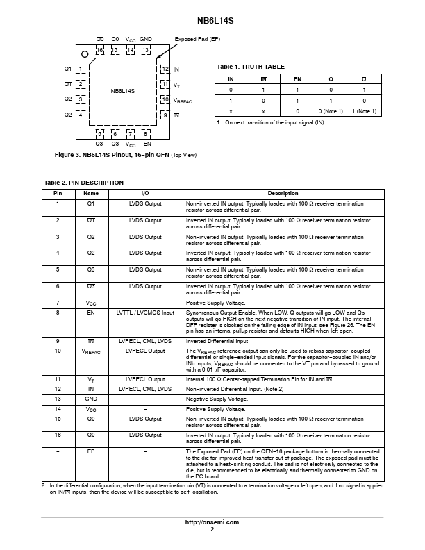
inverted IN output.
Typically loaded with 100 W receiver termination resistor across differential pair.
Inverted IN output.
| Part number | NB6L14S |
|---|---|
| Manufacturer | onsemi |
| File Size | 224.77 KB |
| Description | 2.5V 1:4 AnyLevel Differential Input to LVDS Fanout Buffer/Translator |
| Datasheet |
NB6L14S Datasheet
|
|
|
|
| Part Number | Description | Manufacturer |
|---|---|---|
| NB632 | High Effeciency 4A 24V Synchronous Step-down Converter | MPS |
| NB633 | Synchronous Step-down Converter | MPS |
| NB633EL | Synchronous Step-down Converter | MPS |
| NB636 | 500kHz Synchronous Step-down Converter | MPS |
| NB636DL | 500kHz Synchronous Step-down Converter | MPS |
| Part Number | Description |
|---|---|
| NB6L14 | Differential 1:4 LVPECL Fanout Buffer |
| NB6L14M | Differential 1:4 CML Fanout Buffer |
| NB6L11 | 2.5V / 3.3V MULTILEVEL INPUT TO DIFFERENTIAL LVPECL/LVNECL |
| NB6L11M | Differential CML Fanout Buffer |
| NB6L11S | Input to LVDS Fanout Buffer/Translator |
The following content is an automatically extracted verbatim text from the original manufacturer datasheet and is provided for reference purposes only.