NB3V1102C
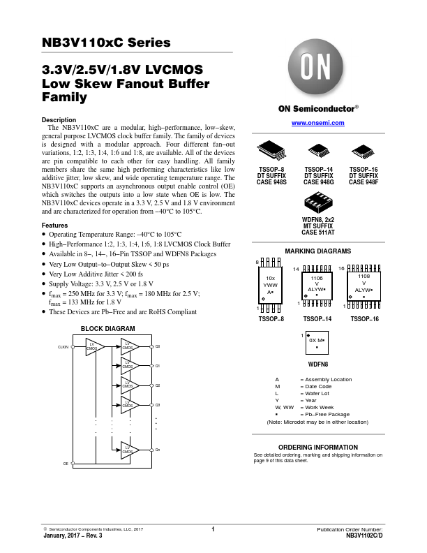
Overview
- Operating Temperature Range: -40°C to 105°C
- High-Performance 1:2, 1:3, 1:4, 1:6, 1:8 LVCMOS Clock Buffer
- Available in 8-, 14-, 16-Pin TSSOP and WDFN8 Packages
- Very Low Output-to-Output Skew < 50 ps
- Very Low Additive Jitter < 200 fs
- Supply Voltage: 3.3 V, 2.5 V or 1.8 V
- fmax = 250 MHz for 3.3 V; fmax = 180 MHz for 2.5 V; fmax = 133 MHz for 1.8 V
- These Devices are Pb-Free and are RoHS Compliant