Datasheet Details
| Part number | NB3M8304C |
|---|---|
| Manufacturer | onsemi |
| File Size | 79.17 KB |
| Description | 3.3V 200 MHz 1:4 LVCMOS/LVTTL Low Skew Fanout Buffer |
| Datasheet |
 NB3M8304C Datasheet NB3M8304C Datasheet
|
|
|
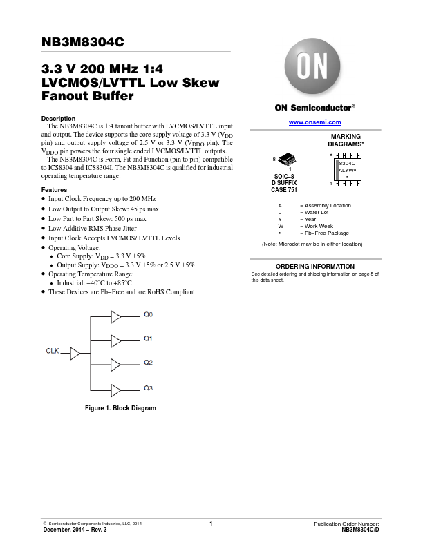
and output.
The device supports the core supply voltage of 3.3 V (VDD pin) and output supply voltage of 2.5 V or 3.3 V (VDDO pin).
The VDDO pin powers the four single ended LVCMOS/LVTTL outputs.
| Part number | NB3M8304C |
|---|---|
| Manufacturer | onsemi |
| File Size | 79.17 KB |
| Description | 3.3V 200 MHz 1:4 LVCMOS/LVTTL Low Skew Fanout Buffer |
| Datasheet |
NB3M8304C Datasheet
|
|
|
|