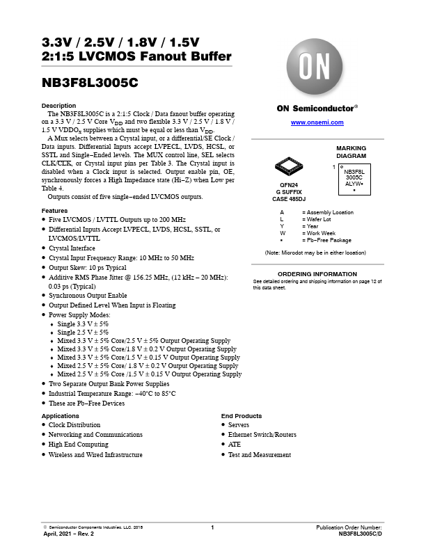
• Part: NB3F8L3005C
  • Description: 2:1:5 LVCMOS Fanout Buffer
  • Manufacturer: onsemi
  • Size: 250.55 KB
Download NB3F8L3005C Datasheet PDF
onsemi
NB3F8L3005C
NB3F8L3005C is 2:1:5 LVCMOS Fanout Buffer manufactured by onsemi.
Description The NB3F8L3005C is a 2:1:5 Clock / Data fanout buffer operating on a 3.3 V / 2.5 V Core VDD and two flexible 3.3 V / 2.5 V / 1.8 V / 1.5 V VDDOx supplies which must be equal or less than VDD. A Mux selects between a Crystal input, or a differential/SE Clock / Data inputs. Differential Inputs accept LVPECL, LVDS, HCSL, or SSTL and Single- Ended levels. The MUX control line, SEL selects CLK/CLK, or Crystal input pins per Table 3. The Crystal input is disabled when a Clock input is selected. Output enable pin, OE, synchronously forces a High Impedance state (Hi- Z) when Low per Table 4. Outputs consist of five single- ended LVCMOS outputs. .onsemi. QFN24 G SUFFIX CASE 485DJ MARKING DIAGRAM 1 NB3F8L 3005C ALYWG G Features - Five LVCMOS / LVTTL Outputs up to 200 MHz - Differential Inputs Accept LVPECL, LVDS, HCSL, SSTL, or LVCMOS/LVTTL - Crystal Interface - Crystal Input Frequency Range: 10 MHz to 50 MHz - Output Skew: 10 ps Typical - Additive RMS Phase Jitter @ 156.25 MHz, (12 k Hz - 20 MHz): 0.03 ps (Typical) - Synchronous Output Enable - Output Defined Level When Input is Floating - Power Supply Modes: - Single 3.3 V ± 5% - Single 2.5 V ± 5% - Mixed 3.3 V ± 5% Core/2.5 V ± 5% Output Operating Supply - Mixed 3.3 V ± 5% Core/1.8 V ± 0.2 V Output Operating Supply - Mixed 3.3 V ± 5% Core/1.5 V ± 0.15 V Output Operating Supply - Mixed 2.5 V ± 5% Core/ 1.8 V ± 0.2 V Output Operating Supply - Mixed 2.5 V ± 5% Core /1.5 V ± 0.15 V Output Operating Supply - Two Separate Output Bank Power Supplies - Industrial Temperature Range: - 40°C to 85°C - These are Pb- Free Devices = Assembly Location = Wafer Lot = Year = Work...