The following content is an automatically extracted verbatim text
from the original manufacturer datasheet and is provided for reference purposes only.
View original datasheet text
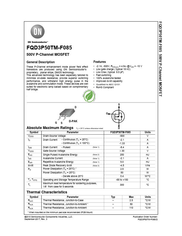
FQD3P50TM-F085 500V P-Channel MOSFET
FQD3P50TM-F085
500V P-Channel MOSFET
General Description
These P-Channel enhancement mode power field effect transistors are produced using ON Semiconductor’s proprietary, planar stripe, DMOS technology. This advanced technology has been especially tailored to minimize on-state resistance, provide superior switching performance, and withstand high energy pulse in the avalanche and commutation mode. These devices are well suited for electronic lamp ballast based on complimentary half bridge.
Features
• -2.1A, -500V, RDS(on) = 4.9Ω @VGS = -10 V • Low gate charge ( typical 18 nC) • Low Crss ( typical 9.
 FQD3P50TM-F085 Datasheet